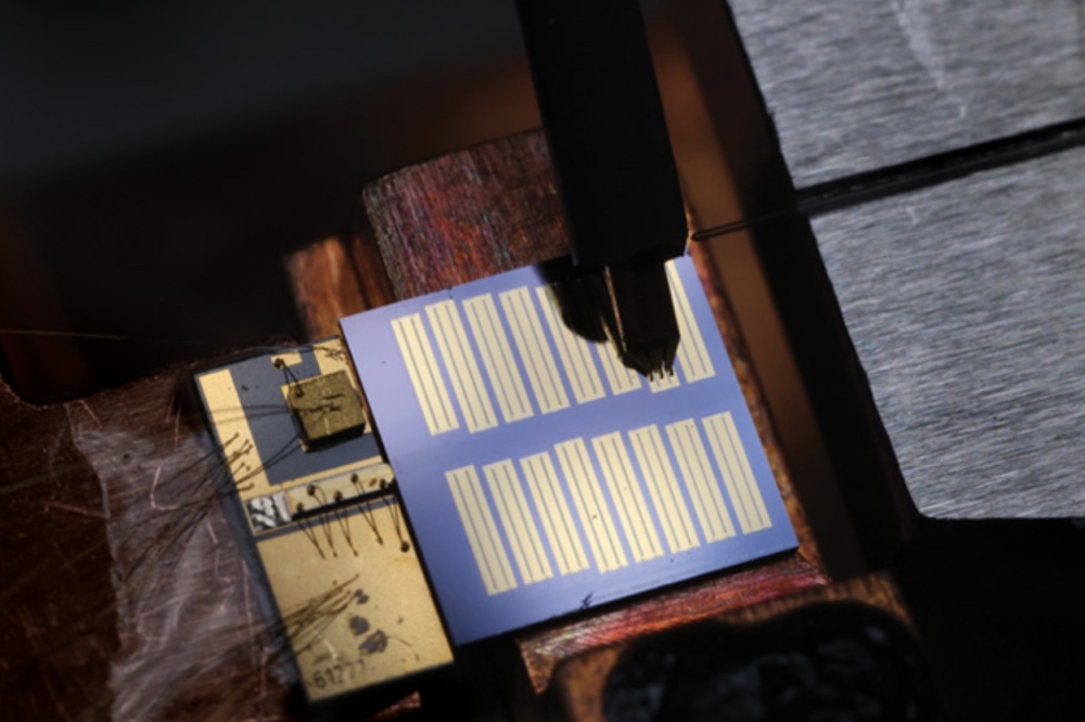
Lumotive on its world-first 2D photonic beamforming chip
Lumotive’s innovation opens new possibilities for optical circuit switching in AI data centers, photonic communications, optical computing and advanced 3D sensing for physical AI.
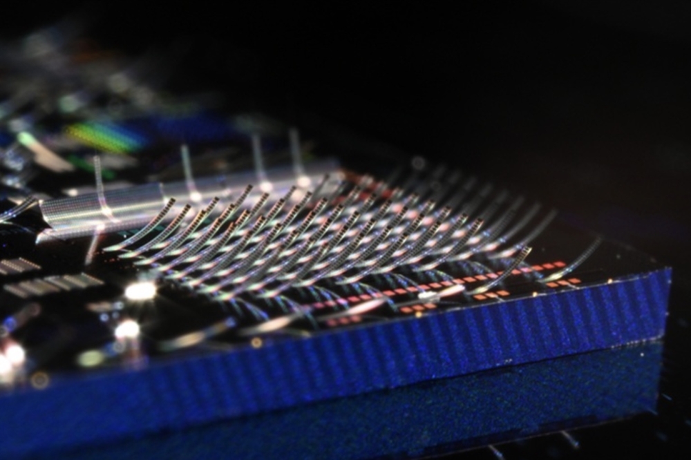
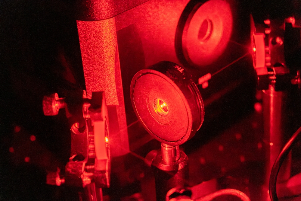
Lumotive has announced a major breakthrough in photonics: the first demonstration of two-dimensional photonic beamforming on a semiconductor chip. The innovation marks a step-change in how light can be controlled, with implications for AI infrastructure, communications, and optical computing.
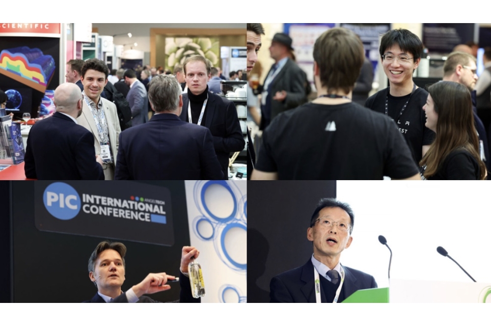
Sarab Chopra, Editor of PIC Magazine, spoke with Sam Heidari, CEO of Lumotive, to understand the significance of this development and what it means for the future of programmable optics.
SC: Can you explain the significance of achieving two-dimensional photonic beamforming on a semiconductor chip?
SH: This is a major milestone for photonics. Just as two-dimensional phased arrays transformed radar and radio by enabling full electronic control of electromagnetic waves, we’ve now demonstrated that same level of control at optical frequencies on a semiconductor chip for the first time. This breakthrough builds on our earlier achievement of delivering the first commercially viable one-dimensional beam-steering system, underscoring our ability to innovate and translate innovation into real-world, scalable products.
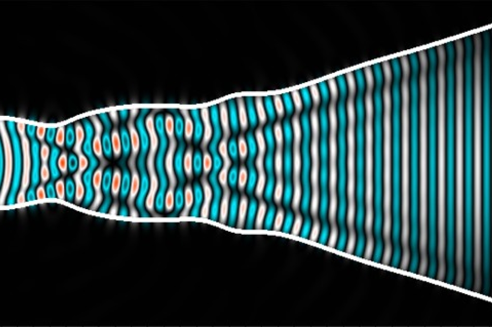
By enabling dynamic, two-dimensional beamforming directly on-chip, we’re turning light from something static into something fully programmable. This unlocks an entirely new class of optical systems: moving beyond fixed optics and mechanical steering to real-time, electronic control with the flexibility of modern computing platforms. It’s a fundamental shift in how optical systems are built, and a critical step toward scaling optical technologies for AI infrastructure and next-generation communications.
SC: How does Lumotive’s LCM™ architecture differ from existing approaches to optical beam steering?
SH: Most existing approaches rely on either mechanical movement or limited, one-dimensional control. Our LCM architecture changes that entirely. It is fully solid-state and software-defined, using nanoscale pixels on a semiconductor chip to precisely control the phase of light across two dimensions. This enables dynamic beam shaping and steering with no moving parts, unlocking a level of precision, speed, reliability, and scalability that hasn’t been possible before.
This integration enables a single chip to replace multiple traditional optical components, such as mirrors, lenses, and beam splitters, while introducing real-time, software-based reconfiguration. The result is a highly integrated, programmable optical platform that fundamentally differentiates itself from conventional approaches and sets a new standard for the industry.
SC: What are the key advantages of software-defined control of light for AI data centre and communications applications?
SH: The biggest advantage is flexibility.
With software-defined optics, you’re not locked into a fixed design. You can dynamically reconfigure how light is used — including steering, shaping, and even correcting for imperfections in real time.
In data centers, that means:
- Any-to-any connectivity without physical reconfiguration
- Continuous wavefront correction and calibration
- Improved coupling efficiency over time
- Higher system reliability and uptime
At a business level, this translates to lower power consumption, better bandwidth utilisation, and longer system life.
SC: How does this breakthrough enable optical circuit switching at scale for next-generation AI infrastructure?
SH: AI infrastructure is pushing networks to their limits. Optical circuit switching has long been seen as a way to enable direct, high-bandwidth connections between compute nodes, but scaling it has been difficult.
What our technology enables is fully electronic beam control in two dimensions, which is critical for scalable switching.
It allows us to build systems that can scale from:
- Compact, rack-level switches (hundreds of ports), to
- Very high-radix systems (thousands to tens of thousands of ports)
That’s what enables flatter network architectures, fewer hops, and significantly better efficiency for large AI clusters.
SC: What role does CMOS compatibility play in accelerating commercial adoption of this technology?
SH: CMOS compatibility is key to making this real. By aligning with established semiconductor manufacturing processes, we can leverage existing infrastructure to scale production, improve yield, and reduce cost. More importantly, it bridges the gap between lab research and real-world deployment by turning this into a manufacturable, commercially viable technology that can be produced reliably, integrated easily, and deployed at the scale required for AI infrastructure.
SC: What are the next steps for Lumotive in bringing programmable photonic semiconductors to market?
SH: Our focus now is execution. We’re translating this breakthrough into our first commercial product, with an initial announcement expected later this year. In parallel, we’re working closely with key ecosystem partners to integrate this technology into real-world systems.
The goal is to move quickly from demonstration to deployment, bringing programmable photonic semiconductors into hyperscale data center environments starting next year. Longer term, we see this as a platform. This is not just one product. It is the foundation for a new class of programmable optical infrastructure.