POET explains hybrid integration, optical engines and chiplet-based PIC development in the AI era

As AI workloads strain copper interconnects, hybrid integration, optical engines, and chiplet-based PICs are emerging as scalable, energy-efficient solutions to power next-generation data centre and hyperscale infrastructure
BY DR SURESH VENKATESAN, EXECUTIVE CHAIRMAN AND CEO, POET TECHNOLOGIES
AS ARTIFICIAL intelligence systems advance toward ever more demanding workloads and sprawling data centre fabrics, the semiconductor industry faces a looming bottleneck in data transfer. Traditional copper interconnects, long in the backbone of server, switch, and GPU communication, are nearing their physical limits for speed, power, and scalability. To sustain the next wave of AI models and hyperscale networking, the industry is pivoting toward photonics.
The ability of light-based signaling to carry vast amounts of data at high speed with far lower energy than electron-based copper traces is pivotal as the AI era accelerates.At the heart of the transformation to increased photonics use are innovative approaches like hybrid integration, optical engines, and chiplet-based photonic integrated circuits (PICs).
How CPO can solve the data transfer bottleneck in the AI revolution
For decades, scaling semiconductor performance relied on Moore’s law — shrinking transistors to pack more gates into a silicon die every two years or less. But as we push into an era of AI accelerators, GPUs, and massive model parallelism, a new constraint has emerged: interconnect bottlenecks. This means that even when individual processing units are powerful, the speed, energy cost, and latency of moving data between them (or memory and other systems) can throttle overall performance.
AI workloads, especially large language models (LLMs) and multimodal systems, are becoming heavier as they are tasked with moving massive amounts of data. Training and inference require constant exchange of information across processors, memory modules, accelerators, and networking stacks. The result? Traditional interconnects begin to falter.
“Though conductive copper interconnect is well understood, it presents fundamental limitations when transmitting data signals at the high frequencies required for modern XPUs in the age of AI,” states PhotonDelta. “In-package and chip-to-chip optical interconnect not only promise to support the computational bandwidth that AI data centres demand, but they can also reduce latency, heat generation, power consumption, and signal degradation.”
Industry voices have emphasized that data transfer bandwidth and energy efficiency are now the key system bottlenecks in AI infrastructure, outpacing even compute core performance. As a result, momentum has been built toward co-packaged optics.
“As hyperscale computing grows and data centre infrastructure evolves, switch designs are shifting toward co-packaged optics (CPO), which embed optical chiplets in the same package as the ASICs (application-specific integrated circuit). CPO approach shortens interconnect lengths, thereby reducing power consumption, while simultaneously enabling a more compact footprint and higher bandwidth density,” writes Pingfan Wu, Senior Technical Director at Futurewei Technologies, in ComSoc Technology News.
Optical links and photonic techniques offer orders of magnitude higher data densities and dramatically lower energy per bit than traditional solutions. For example, PICs are gaining traction because of their promise to replace problematic electrical interconnects with optical links, delivering high bandwidth with low latency and power. But traditional silicon photonic devices require complex fabrication and expensive packaging, which has limited the adoption of PICs. And while optical signaling is inherently superior at scale, getting photonics integrated with existing electronic workflows — at volume and low cost — has been one of the industry’s largest hurdles this decade.
Cost and performance advantages of hybrid integration
Now, hybrid integration has matured. It represents a structural shift in how photonic systems are built and scaled. At its core, hybrid integration brings together components made from different materials into a single package. This design typically enables automated wafer-scale assembly (rather than manual alignment of discrete parts), and chiplet-level packaging where photonics and electronics operate in concert in one high-speed subsystem.
Hybrid integration allows for flexibility in design and manufacturing. Large monolithic dies suffer disproportionately from defects, where a single flaw can render an entire chip unusable. But chiplet-based hybrid integration mitigates that risk by breaking functionality into smaller, known-good dies that can be tested independently before assembly. According to a 2024 McKinsey analysis on advanced packaging, chiplet-based architectures can improve effective yield by more than 30% while simultaneously shortening development cycles. The yield advantage directly translates into lower cost per bit— a critical metric for AI networking infrastructure.
Hybrid integration also reduces cost by simplifying packaging and assembly. Conventional photonic modules often require active alignment, manual fibre attachment, and labour-intensive testing. Wafer-scale hybrid integration enables passive alignment and parallel assembly, dramatically reducing manufacturing time and capital expenditure.
On the performance side, hybrid integration shortens electrical interconnect lengths and enables tighter coupling between photonics and electronics. By placing drivers, modulators, and detectors within the same package, signal integrity improves while power consumption drops. The result is lower energy per bit, higher bandwidth density, and reduced latency—key requirements for AI training clusters where microseconds of delay can cascade into significant efficiency losses at scale.
With added efficiency, hybrid integration also accelerates time-to-market, which is essential in an AI landscape where network speeds are advancing from 400G to 800G to 1.6T in rapid succession. As LightCounting has observed, “The economics of optical networking increasingly favor platforms that can scale bandwidth without scaling complexity.”
For hyperscalers and AI system architects under pressure to deploy ever-higher bandwidth at sustainable cost and power levels; hybrid integration is not merely an incremental improvement—it is a foundational enabler of next-generation AI infrastructure.
Why chiplets have risen to the forefront of photonics design
Getting to this point in the evolution of hybrid integration has not been simple. Breakthroughs in photonic integration have taken place because increased research and development has led to an understanding of why light performs so well at higher speeds. The challenge recently has been to harness its abilities. Photons travel with no resistive loss (a difference from electrons, which do have resistive loss when moving through copper); optical waveguides and fibers enable bandwidth densities unachievable with metal traces; and optical signaling reduces heat and cross-talk.
As the industry unlocks more potential from hybrid integration, chiplet design has emerged as a leading option to solve the data-transfer bottleneck. Increasingly employed to mix best- of-breed components in photonics, chiplets enable yield improvements because they have smaller dies than large monolithic chips and more flexibility. Chiplets can be configured in various combinations for targeted applications, and they can also use a range of materials.

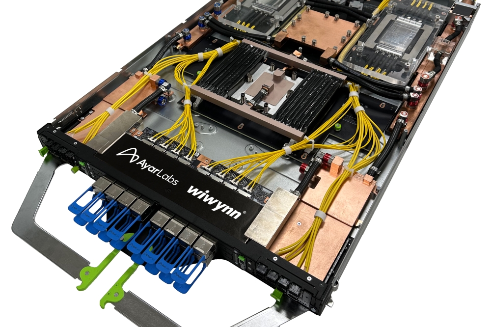
The deployment of optical engines, which are a commercially viable form of chiplets, has been one of the first moves by the industry to usher hybrid-integrated subsystems into the marketplace. Optical engines generally combine electrical drivers, high-speed modulators, lasers, photodetectors, waveguides, and other components. These engines act as the bridge between electrical processing and optical signaling, converting high-speed electronic data into light and back.
Optical engines deliver advantages including:
- High data rates — optical channels can scale beyond terabits per second per module.
- Lower energy per bit — light propagation in waveguides incurs minimal loss and heat to deliver this crucial metric for AI hardware manufacturers.
- Reduced latency — light travels faster with fewer intermediate conversions.
- Scalability — optical links extend over meters or kilometers with low signal degradation.
These capabilities make optical engines ideal for AI cluster and ultra-fast networking, where massive amounts of data move continuously and unpredictably.
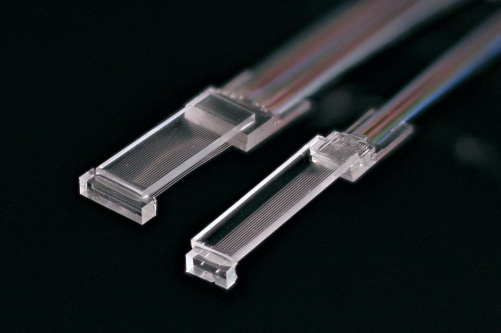
Optical interposer technology is a key solution for the AI era
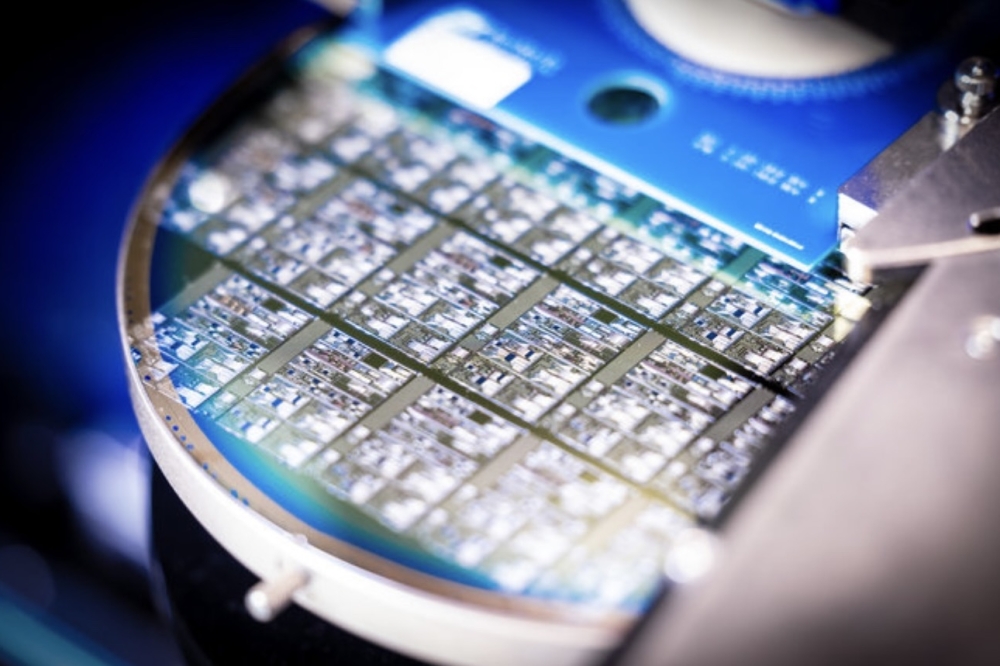
Among the leading technologies used in the design and assembly of optical engines is the optical interposer. An optical interposer is attractive to the industry because of its CMOS compatibility, allowing conventional semiconductor fabrication processes to be used in building photonic systems at scale. This attribute enables low-cost, high-throughput assembly and testing across hundreds of devices simultaneously.
POET Technologies’ Optical Interposer™ was created to be a platform technology that can power the next generation of compute devices. Using a “semiconductorization of photonics” approach that combines electronics and photonics at a wafer scale, POET’s optical interposer dramatically reduces assembly complexity and cost. By embedding low-loss optical waveguides into silicon interposer with integrated electrical traces, the platform enables seamless integration of diverse components — lasers, detectors, modulators, and driver electronics — into fully realized optical engines.
In 2025, POET proved the commercial credibility of the platform as its partnerships with a number of industry leaders matured. Among its core products is POET Teralight™, a line of 1.6 Tbps transmit and receive optical engines that illustrate scalability to next-generation speeds and longer reaches suitable for AI systems networks and hyperscale data centers. The Teralight engines support emerging high-speed standards and reduce assembly steps by eliminating traditional wire bonding and active alignment. The Teralight engines have garnered industry recognition, winning multiple competitions, including most recently at China’s Infostone (ICCSZ) Awards, where it was named Product Innovation of the Year during a ceremony on January 16, 2026.
By merging hybrid integration with chiplet-scale design, POET’s approach addresses key industry pain points — cost, scalability, and performance, enabling optical interconnect architectures ready for the AI era.
Together, hybrid integration, optical engines, and chiplet-based PICs deliver a reliable path forward for photonic interconnects that sidestep the power-heavy limitations of copper — enabling AI data applications to grow without being choked by electrical bottlenecks. How to effectively power the AI revolution has been a conundrum for the industry in recent years, but viable solutions have appeared and, bit by bit, are becoming the foundation of exciting new system designs and light-based interconnect solutions.