CPO advances AI infrastructure scaling

Integration of photonics with computing is set to overcome bandwidth and energy limits in next-generation data centres.
The rapid growth of artificial intelligence is accelerating the shift toward large-scale, distributed compute architectures, driving demand for new interconnect technologies such as co-packaged optics (CPO).
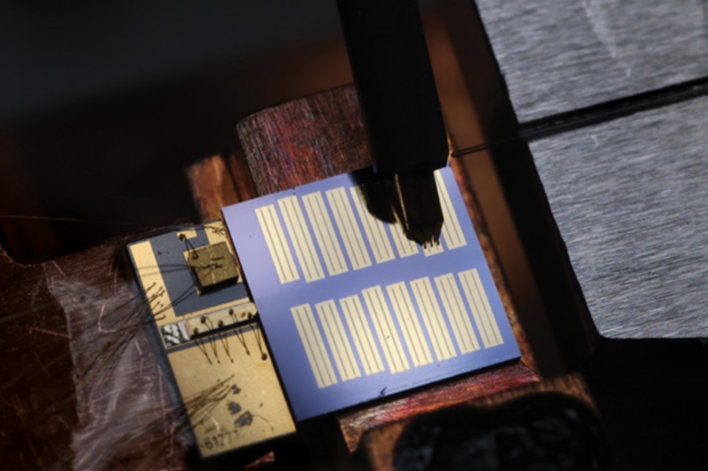
CPO integrates optical engines closer to switch and processor chips, replacing traditional front-panel transceivers to reduce signal loss, improve bandwidth density, and lower power consumption. This approach is emerging as a key enabler for scaling AI infrastructure, particularly as copper interconnects reach their physical limits.
Recent advances in electronic and photonic integration have already delivered significant gains, including a 64-fold increase in bandwidth density and a fivefold improvement in energy efficiency over the past five years. However, challenges remain in bringing CPO to high-volume manufacturing.
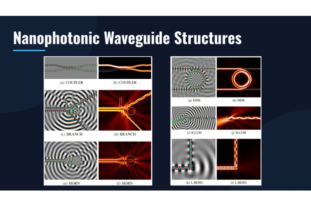
A key issue is the mismatch between the bandwidth density of AI chiplets and current optical interconnects, highlighting the need for more compact and scalable photonic integrated circuits. Fiber array design, wavelength stability, and thermal management also present ongoing technical hurdles.
Manufacturing complexity is another barrier, with CPO systems requiring the integration of lasers, photonic circuits, and fiber arrays across multiple process nodes.
Active alignment techniques, while necessary for performance, can limit throughput and increase costs. In addition, conventional permanent bonding methods reduce repairability, prompting industry efforts to develop detachable fiber array solutions.
Testing and yield optimisation are also critical concerns. The adoption of “known-good” optical engines, verified through wafer-level testing prior to final assembly, is seen as essential for improving manufacturing efficiency.
However, not all integration approaches are compatible with current testing methods, particularly in advanced 3D configurations.
Despite these challenges, co-packaged optics is widely viewed as a cornerstone technology for future AI and hyperscale data centre systems.
Continued progress will depend on close collaboration across the semiconductor and photonics ecosystem, spanning design, packaging, and system integration.