MIT develops ‘Ski Jump’ photonic chips
Researchers at MIT have created microscopic curved structures that allow photonic chips to project thousands of controlled laser beams into free space, potentially enabling advances in quantum computing, displays, and lidar.
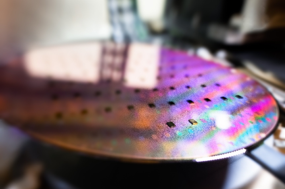
Researchers at the Massachusetts Institute of Technology (MIT) have developed a new photonic chip architecture that enables light to be efficiently projected from on-chip optical waveguides into free space. The innovation could support new applications ranging from high-resolution displays to scalable quantum computing systems.
Photonic chips offer significant advantages over electronic chips in terms of communication speed and bandwidth. However, one long-standing challenge has been efficiently transmitting light off the chip. In most photonic circuits, light remains confined within waveguides, making it difficult to interact with external systems.
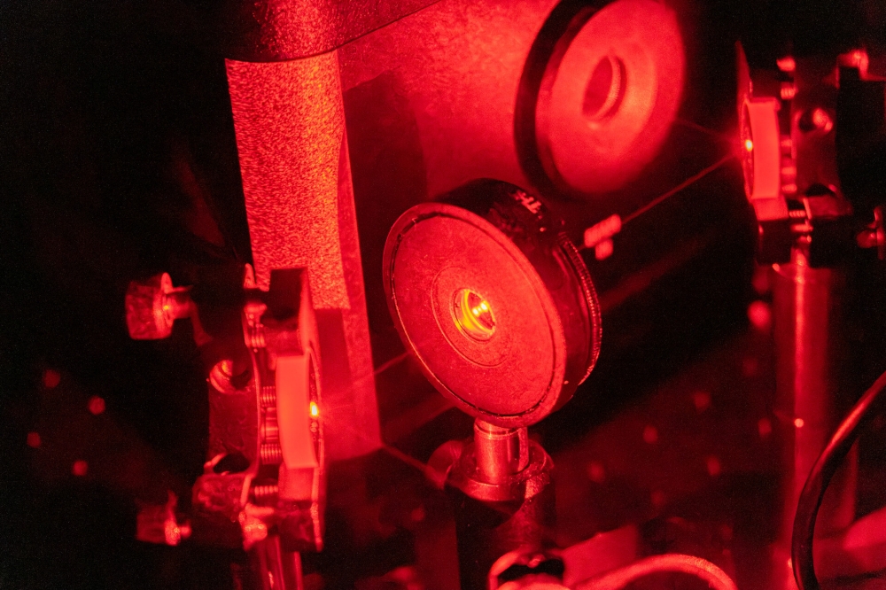
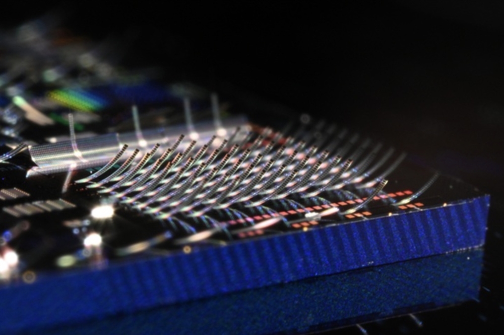
To address this limitation, a research team led by Dirk Englund at MIT has developed arrays of microscopic structures that curve upward from the surface of the chip. These structures resemble tiny ski jumps and allow light traveling through the chip’s optical waveguides to be emitted outward into free space.
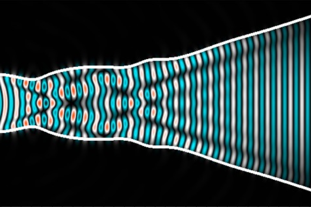
The team demonstrated that thousands of these structures can be controlled simultaneously, allowing the chip to generate large arrays of precisely directed laser beams. Using this platform, the researchers were able to project detailed full-colour images measuring roughly half the size of a grain of salt.
According to co-lead author Henry Wen, the technology provides a new way to bridge the gap between integrated photonics and the free-space optical world. By controlling how light exits the chip, the system can create multiple laser beams that can interact directly with external devices or environments.
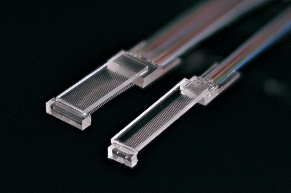
The device is fabricated using a two-layer material structure made from silicon nitride and aluminium nitride. Because the two materials expand and contract differently when cooled after fabrication, the resulting strain causes the structures to bend upward. This controlled curvature forms the tiny “ski jump” emitters that direct light off the chip.
Light from on-chip waveguides is routed to these structures, where modulators control when and how beams are emitted. The system can rapidly switch and steer light while maintaining stable beam patterns.
The research is part of the Quantum Moonshot Program, a collaboration involving MIT, the University of Colorado Boulder, the MITRE Corporation, and Sandia National Laboratories. The initiative aims to develop new quantum computing platforms based on diamond-based quantum bits.
In these systems, qubits are controlled using laser beams. However, scaling quantum computers to millions of qubits would require the ability to manipulate large numbers of beams simultaneously. The new photonic platform could provide a scalable method for doing so.
Beyond quantum computing, the researchers say the technology could enable compact lidar sensors, high-resolution micro-displays for augmented reality devices, and faster laser-based 3D printing systems.
Future work will focus on scaling the technology to larger arrays and testing the long-term performance and reliability of the devices.