PICs enter bioreactors: what it takes to monitor cell growth in real-time
InSpek’s PIC sensors enable real-time bioprocess monitoring on a scale previously unachievable. But pharmaceutical manufacturing demands completely novel engineering solutions in photonic integration
BY IVAN-LAZAR BUNDALO, CTO INSPEK
EVERY DAY at pharmaceutical facilities worldwide, a scientist samples a 1-litre glass bioreactor containing brownish liquid. Inside: valuable microorganisms or cells and their entire microbiome. The sample goes to an analytical lab. Then comes the wait: 4 to 24 hours for results.
Meanwhile, life in the original container continues. If culture conditions drift, that fact remains unknown. Contamination, stress, oxygen deprivation - all stay undetected until the run fails or a scientist acts in time. Each failed batch can cost millions of euros. For vaccines and cancer treatments, failures delay patient access by months. Regulatory approval can slip by years.
The irony is stark. Modern medicine can fend off pandemics and fight many cancers. Yet the factories making these drugs operate with primitive tools, unable to see inside bioreactors in real time – a remarkable feat in itself. Think of it like this: running a bioprocess is like driving a car through a city but seeing your speed and position only every 10 seconds, with the newest data already 10 seconds old.
If this problem gets solved, the impact extends beyond factory floors. Faster process optimisation could shorten drug development timelines by months. Higher yields would reduce manufacturing costs. More immediately, reducing batch failures means fewer drug shortages, a chronic problem in biopharmaceuticals where supply barely meets demand.
InSpek, a Parisian startup, is miniaturising optical spectroscopic methods onto a photonic chip. Real-time multiparameter sensing at this scale changes bioprocessing economics. These are multibillion- euro industries where even small optimisations are worth millions. The challenge is that pharmaceutical manufacturing demands solving problems telecommunications photonics never faced.
A patent for seeing the invisible
InSpek was founded by Jérôme Michon, who brought the technology from his MIT PhD back to Paris. The company has 14 full-time staff, including 6 PhDs specialised in optics, biotech and AI. Unusually for a French startup, it has more foreigners than French people. The company raised €3.5m in seed funding two years ago and is preparing for a Series A round this year. It has backing from the European Union via the EIC Accelerator, the world’s biggest and most prestigious startup grant.

InSpek is based in Paris and is run by an international team of PhDs and engineers in Optics, Bioprocessing and AI.
Why is InSpek first in this domain? Sensing weak optical signals on a chip generates lots of background noise. InSpek started with a patent to clear that noise, becoming the first company able to detect these faint scattering signals in a photonic integrated circuit, in possibly the most complicated spectroscopic method called Raman. Incumbents in the bulk optics sensor business are usually unaware of integrated photonics. Though both involve optics, integrated photonics operates on very different physics, not easily translatable from bench-scale instruments to chips.
Driving blind through the bioprocess
The problem InSpek is tackling runs deep. Two out of three biopharmaceutical processes fail during scale-up. Nine out of ten non-pharmaceutical bioprocesses fail for the same reason. Complexity increases with volume.
Current sensors are inadequate. Electrochemical sensors measure only one analyte and drift over time, giving unreliable readings. Established optical sensing methods use bulk optics, which makes them bulky and expensive. They quickly occupy scarce bioreactor ports and represent a massive cumulative cost when multiple parameters need monitoring.
There is also a contamination paradox. Each time something enters a bioprocess, failure risk increases. The biopharmaceutical industry is terrified of contamination and often prefers slow, blind processes over having multiple sensors with attendant risk.
What’s needed to start with is a pen-sized probe measuring multiple analytes simultaneously through a single standard port. PICs make this possible because they are tiny and cheap at scale. They also enable something the industry increasingly wants: single-use technologies. Counterintuitively, sterilising reusable sensors multiple times has a bigger carbon footprint than sterilising disposable sensors once, and using more of them. Only PICs make single-use sensors economically viable.
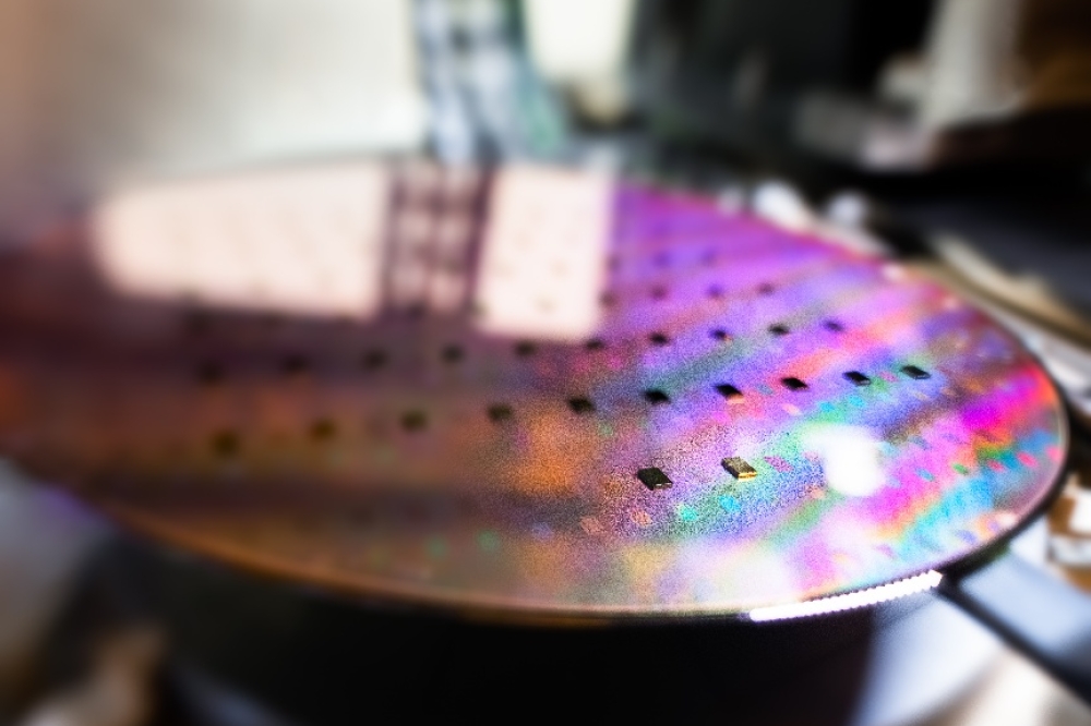
Silicon nitride for a broad spectrum
Most photonic chips since 1985 were optimised for one goal: transmit data through fibre-optic cables at 1550 nanometres, cheaply and over long distances. Silicon photonics excels at that wavelength, so the industry evolved there.
Bioprocess spectroscopy demands something different: wavelengths from 400 to 1000 nanometres. Raman scattering spans 800 to 1000nm. Fluorescence-based pH and oxygen sensing sits near 400nm. Temperature and biomass measurements fall in between. Silicon photonics fails below 800nm, as the material becomes opaque.
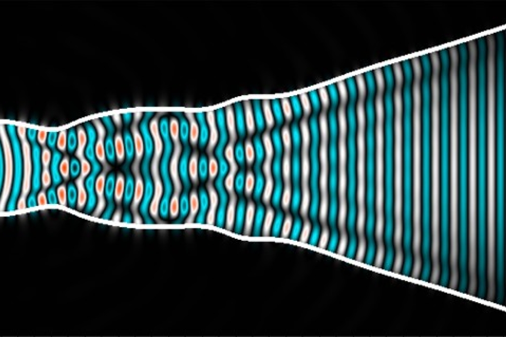
Remaining platform options include silicon nitride, aluminium oxide and lithium niobate. InSpek works with multiple, driven by mature ecosystem, favourable competitive landscape and growing potential of platforms.
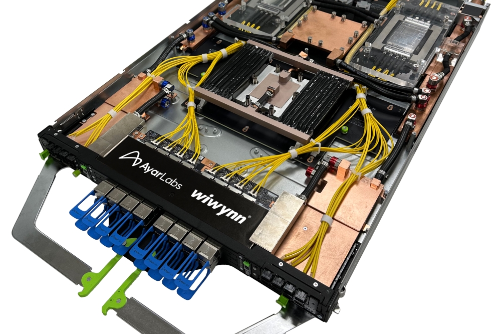
The company’s chips are passive. External lasers and spectrometers do the active work. This decision brings several benefits. As laser and spectrometer technology improves, InSpek’s sensors improve too. Problems are decoupled. Packaging becomes simpler. The alternative, integrating multiple wavelength sources onto one active chip, would be extremely difficult.

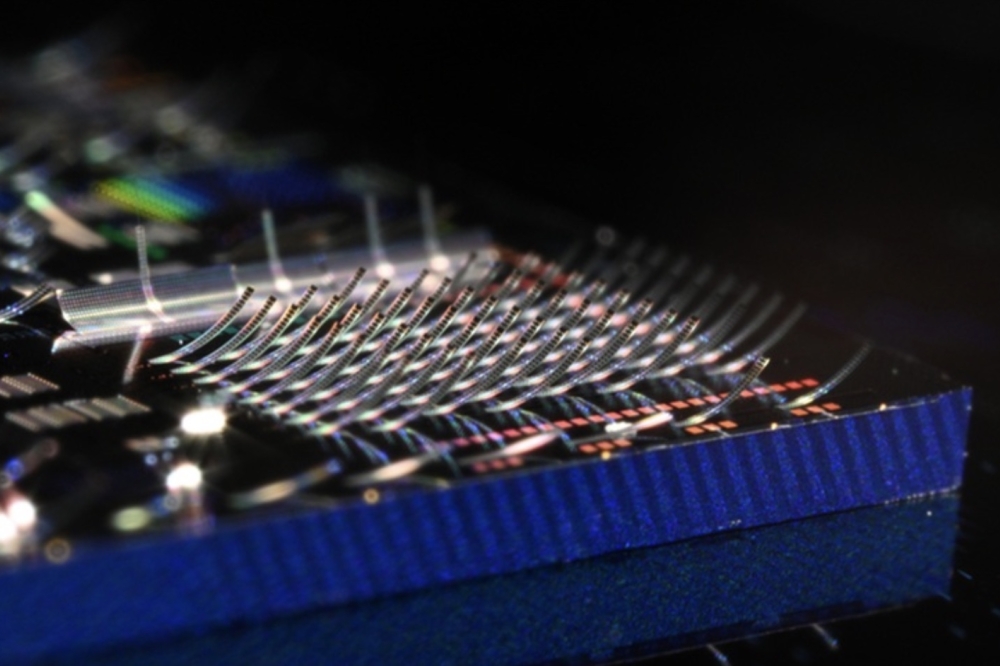
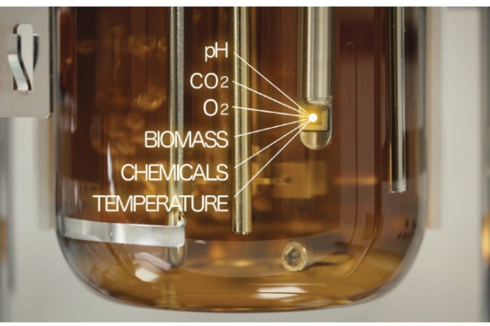
InSpek’s technology grows with market, as the best lasers, spectrometers and other components are decoupled from chip-based sensing technology. One Optical Control Unit (OCU - box in the centre) can monitor multiple probes in different bioreactors.
The challenge is nonetheless impressive. Integrated photonics is difficult even in its “home territory” of telecommunications. InSpek is attempting to drag it into bioprocessing for the first time. Whether a technology optimised for data transmission cables can survive radiation, heat, chemicals and biofilm remains to be answered. Yet InSpek’s bet is that the timing has never been better. The company is piggybacking on decades of telecom photonics development. Silicon nitride foundries matured only in the past decade. Supply chains that didn’t exist 10 years ago are now established. Edge couplers, packaging techniques, design tools exist because telecom companies spent billions perfecting them. InSpek need not invent photonic integration from scratch; they must adapt it. The advantages, they claim, are worth the difficulty.
Packaging takes centre stage
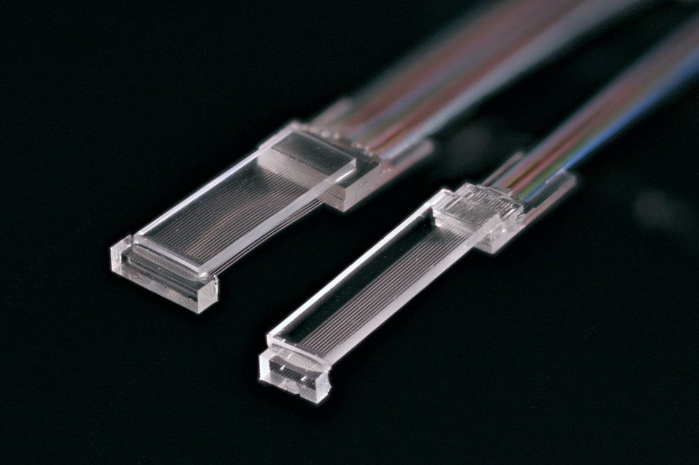
A known problem in the PIC industry is that chip-making represents 40% of the challenge, packaging the other 60%. This is where the team’s difficulties become uniquely severe. Some wonder whether photonics, optimised for telecom over decades, is mature enough to be bent to bioprocessing’s messy demands. Standard approach: plug a fibre array onto the chip using epoxy. It works and survives industrial conditions. Companies have done this for 30 years in telecommunications. InSpek’s packaging requirements are driven by three factors: broadband coupling, packaging losses and sterilisation resistance.
Broadband coupling creates the first headache. As InSpek’s wavelength requirements span visible to near-infrared, edge couplers work best. Standard adhesives for optical packaging require low shrinkage and thermal post-cure to ensure shaded areas cure properly. Most epoxies are not transparent down to 400nm. Amongst the few that are, most suffer rapid photodegradation. The effect, often seen as yellowing and darkening, can appear even after short exposure.
The team explored alternatives such as epoxy-free packaging. Each approach involves trade-offs. Some are expensive, some fragile, some introduce new problems hard to assess. Looking back, it is difficult to see shortcuts that could have been taken when the requirements list is so exhaustive. This explains why InSpek has been accumulating knowledge through multiple packaging projects. Sterilisation survival presents a different taste of tough challenge. Before a bioreactor probe is used, it must be sterilised. Industry standard for single-use applications is gamma ray irradiation at 25 to 55 kilograys. Some multi-use facilities use autoclaving instead: 140°C steam under high pressure for 15 to 20 minutes. Chemical Clean-In-Place (CIP) sterilisation using diluted sodium hydroxide is also used.
All three methods are destructive to many materials. Radiation damages polymer molecules, creating free radicals that break chemical bonds. Material darkens, refractive index shifts, and adhesive becomes brittle. Heat creates a thermal expansion mismatch between dissimilar materials and breaks polymer bonds. Chemical sterilisation eats into materials. Repeated cycles cause microscopic cracking and delamination. Dosing variability, especially with gamma irradiation, makes validation harder still.

Packaging for bioprocess monitoring requires tolerating radiation, high temperature steam and harsh chemicals.
Biofouling adds a third dimension. Once a fully operational sensing probe sits inside a bioprocess for the typical two weeks (some run longer), biofilm forms. This combination of dead and live cells creates a slimy layer on everything, including sensors.
The layer can block sensors from seeing what happens in the bioreactor. Combinations of coatings, electrical and mechanical tools mitigate the process and extend sensor lifetime. InSpek’s packaging solutions address these challenges through material selection, smart design and protective coatings.

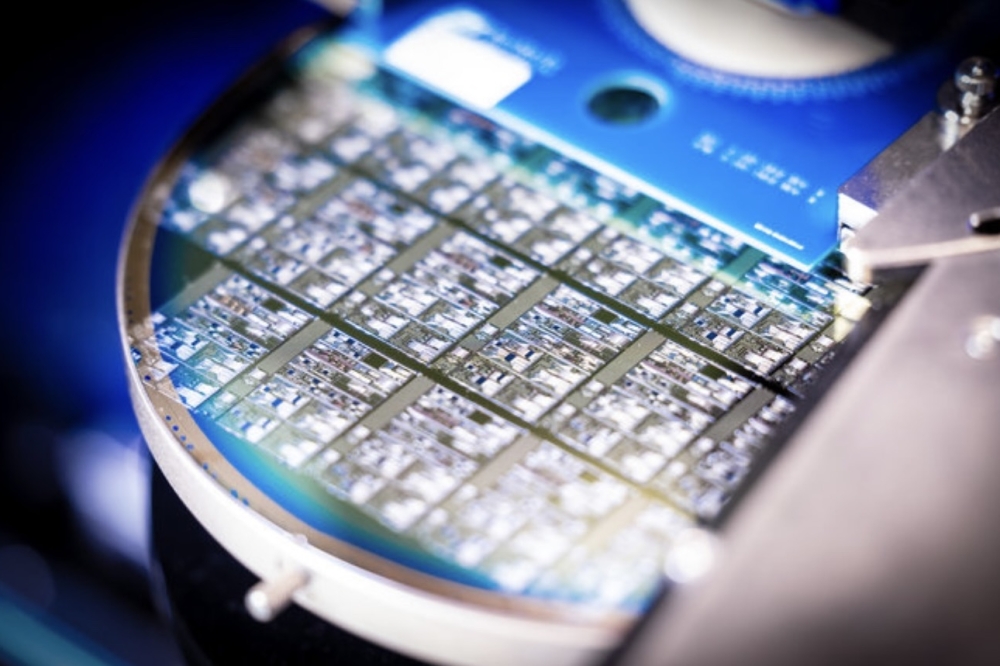
Having multiple sensors on one chip demands visible to IR spectra handling on one PIC, and one probe.
Rhythm of 3 tape-outs per year
Startups face a dilemma. They must iterate quickly to reach market, but in deep-tech integrated photonics entrepreneurship, each chip run costs hundreds of thousands of euros. InSpek’s rhythm: 3 runs per year in 4-month cycles. Design in month one. Fabricate in months two and three. Test, package and analyse in month four, then restart.
This pace is fast compared to typical PIC startups but slow compared to established semiconductor companies doing multiple iterations at a massive scale. These four-month deadlines set the tempo for everything else. Coordination must be excellent; otherwise, the data needed for the next iteration fails to reach designers. An extremely costly mistake.
One sign of startup maturity is logistics diversification. For InSpek this came as a requirement from investors. At least one backup foundry, one backup packaging partner, one backup contract manufacturing organization for whatever work happens externally. Because packaging is so critical, InSpek works with no less than 4 different partners, in addition to their own in-house packaging abilities.

The company’s value was recognised and supported by multiple investors, as well as the European Union. Pictured Jerome Michon, CEO (left), and Ivan-Lazar Bundalo, CTO (right).
Early customers and disruption
InSpek is not launching a finished, perfect product. Instead, the company pursues early deployments in academic labs and smaller facilities - customers willing to tolerate maturing early versions in exchange for being the first to use novel technology.
Real-world data shapes the product faster than internal R&D alone. One concrete example: collaboration with URD ABI showed a 2x yield improvement with InSpek’s technology in production of p-coumaric acid, an important biochemical for the cosmetics industry. Partnerships with some of the biggest companies in the biotech field signal serious interest.
The economics are compelling. The bioprocessing equipment market is massive. Production costs for InSpek’s chips plus packaging rival bulk optics at low scales, coming in at a few hundred euros. At higher volumes, costs drop significantly by leveraging microelectronics-scale economics. The target: below €100 at scale.
The business model focuses on three segments: reusable sensors for multi-use facilities, single-use sensors for disposable bioreactors, and AI data modelling and optimisation services.
Incumbent sensor makers, accustomed to selling expensive bulk optics probes, face disruption. Integrated photonics operates on physics unfamiliar to traditional optics engineers, creating barriers to entry. This is an advantage, as by the time bulk optics companies recognise the potential, InSpek may have an insurmountable lead in chip- based sensing.
Regulatory hurdles exist but are manageable. The pathway is cytotoxicity-based, less stringent than medical device regulation but tough, nonetheless. The bigger challenge is industry reluctance to adopt new technologies, driven by quality requirements and high safety standards. This will not happen overnight, InSpek is in for the long term.
As for most PIC technologies, the central risk remains packaging. If costs stay high or sterilisation proves unreliable at scale, the economics could collapse. Everything else looks promising. InSpek’s vision extends beyond just sensing bioprocesses. Chemistry is a massive market, but there’s something even bigger out there. With unprecedented data volumes, the company wants to enable tight process control using AI. Current focus is on yeast-based fermentation. The future target: monoclonal antibodies for treating major diseases, and advanced AI helper for whatever biotechnological process imaginable.
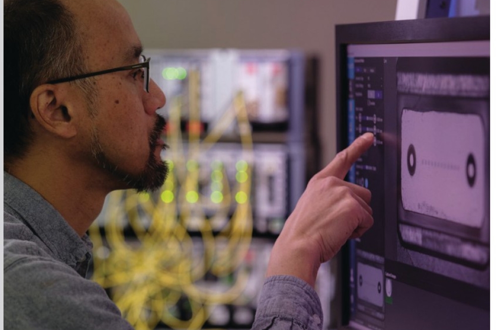
 InSpek’s multiparameter chips enable AI-driven real-time bioprocess optimization
The bioprocessing equipment market is worth billions. Optimisations are worth millions. InSpek’s knowledge in adapting photonics to bioprocessing’s brutal conditions - radiation, heat, chemicals, biofilm - may prove its deepest competitive advantage. Perhaps one day, bioreactor operators will monitor their drug factories with the same precision we now track the pandemics those factories help fight. The primitive tools won’t stay primitive for long.