Eindhoven starts 6-in InP wafer facility

New pilot line aims to scale indium phosphide photonic chip manufacturing for AI, 6G and datacenter applications.
Construction has begun on a new industrial facility in Eindhoven to produce photonic chips on 6-inch indium phosphide wafers, marking a major step toward scaling European photonic integrated circuit manufacturing.
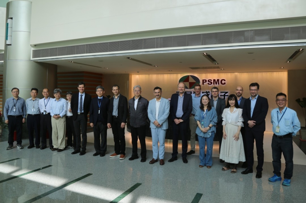
The project is led by the Netherlands Organisation for Applied Scientific Research (TNO) in collaboration with High Tech Campus Eindhoven and forms part of the broader PIXEurope consortium. The initiative is supported by a €150 million investment under the European Chips Act.
Partners in the project include Eindhoven University of Technology, PhotonDelta and SMART Photonics, intending to link research and development with scalable industrial production of photonic integrated circuits.
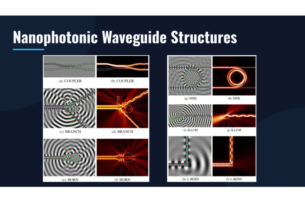
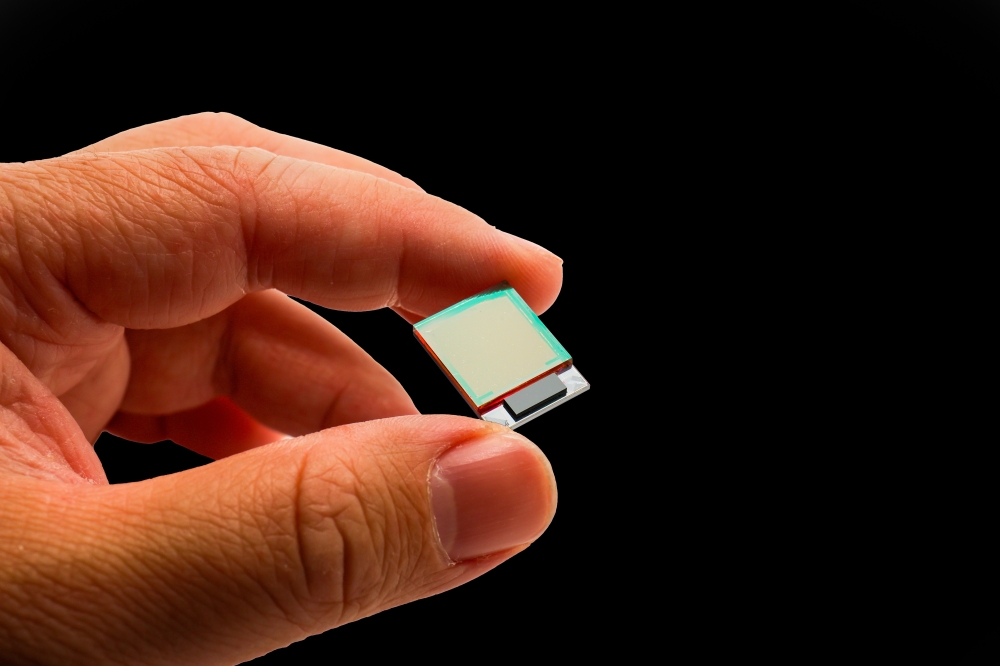
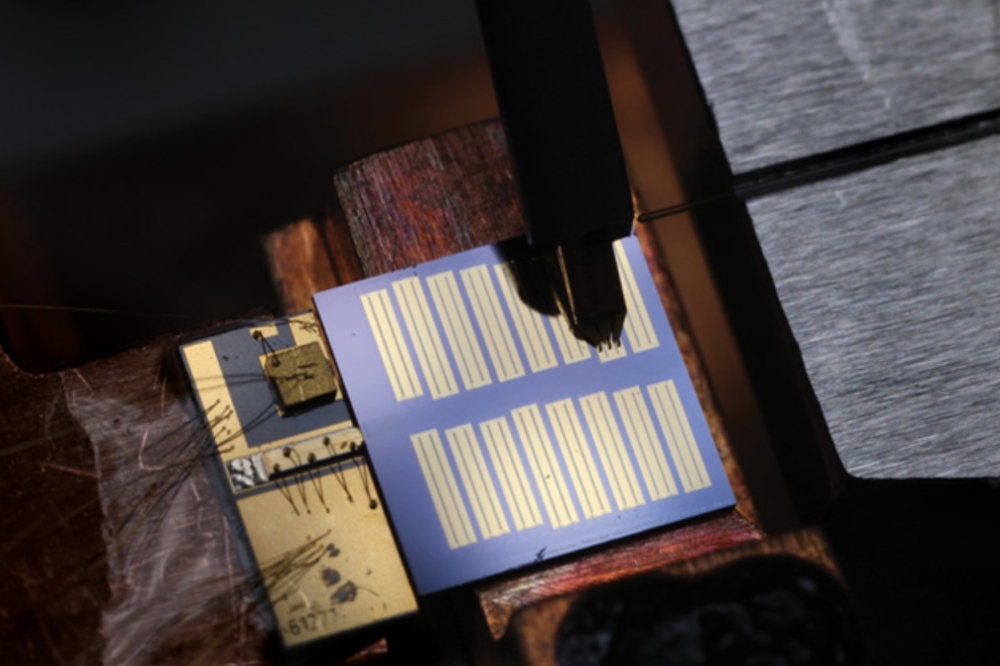
The new facility is expected to be the world’s first dedicated 6-inch indium phosphide wafer production line, enabling higher-volume manufacturing of photonic chips used in applications such as AI data centres, 6G communications, supercomputing and medical technologies.
Plans for the pilot line were first announced in 2024, with detailed development plans revealed in 2025. The project aims to accelerate the transition from research prototypes to commercially deployable photonic technologies in Europe.
The move also reflects growing global competition in InP manufacturing. Coherent has also announced efforts to establish 6-inch indium phosphide wafer production at its facilities in Texas and Sweden.