How co‑packaged optics (CPO) is changing the game in optical testing
By Matthew Adams, Director of Product Line Management, Viavi Solutions
Executive summary
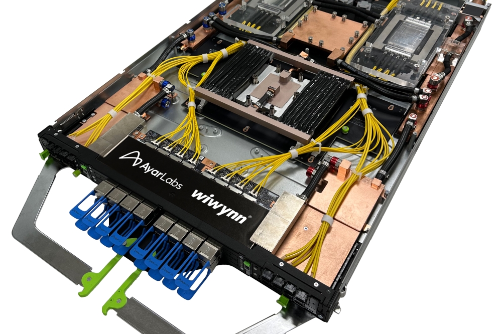
CO‑PACKAGED OPTIC (CPO) based designs promise dramatic gains in bandwidth density and power efficiency for next‑generation switching by moving optical engines adjacent to the switch ASIC. This well‑known architectural shift reduces high speed electrical trace lengths and board‑level electrical losses, but it also reshapes test and measurement from the optical silicon on out: lasers move out of the PIC into external, field‑replaceable modules, light is split across many channels, and the bar rises for source power, linewidth stability, and parametric test rigor.
The Optical Internetworking Forum’s External Laser Small Form‑Factor Pluggable (ELSFP) implementation agreement standardizes this model and enables high‑power, multi‑channel CW delivery inside the chassis via blind‑mate optics—fundamentally altering how designers and manufacturing lines emulate and validate light sources and scale out test to manage the number of parallel optical paths. Both deeply impact on how CPO engines are tested.
The CPO impact on test and measurement
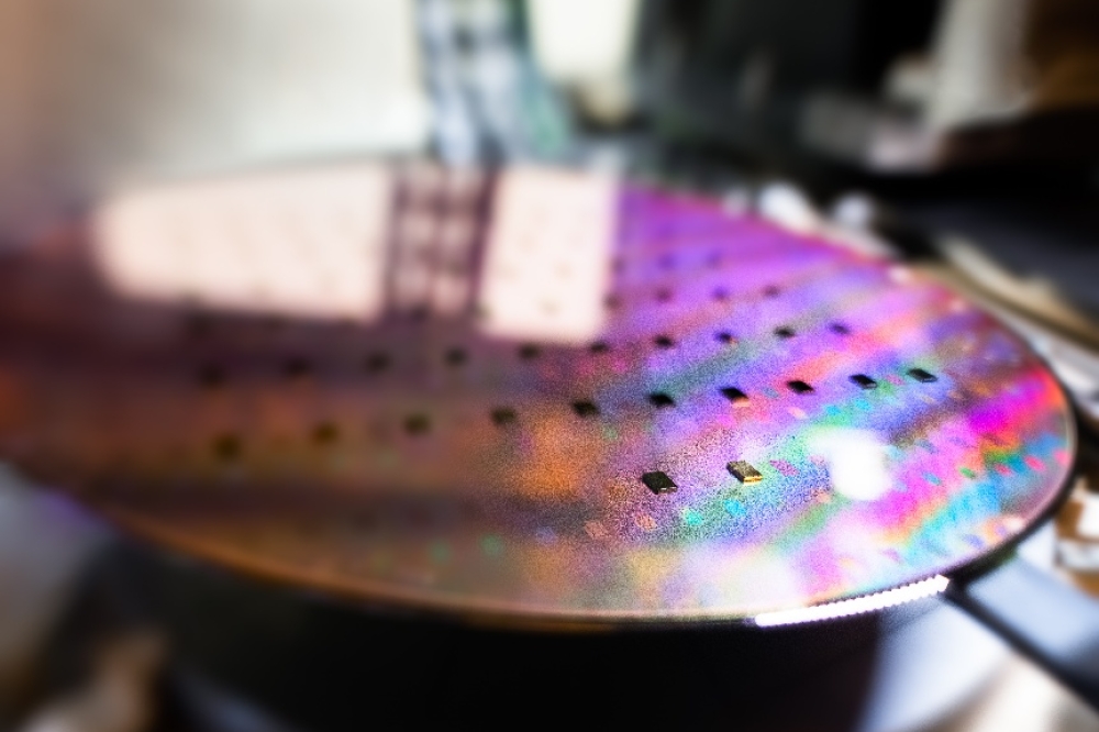
CPO integrates silicon‑photonics (SiPh) optical engines next to the switch ASIC, replacing long, lossy electrical traces with short connections that mitigate channel loss and power‑hungry equalization. As lane counts and radix grow to meet AI fabrics, CPO introduces new test surfaces and denser optical interfaces compared to pluggable modules: Silicon photonic optical interfaces, ultra‑high density fibre management, and board‑level laser distribution and control. For SiPh, CPO is a natural evolution— modulators, filters, and monitors are densely integrated on wafer, and on‑package placement tightens control of coupling, thermal behavior, and telemetry—yet it elevates requirements for external laser quality during both characterization and production test along with the number of transmit and receiver ports to be characterized.
The external laser and the OIF ELSFP
The OIF ELSFP Implementation Agreement defines a faceplate‑pluggable, blind‑mate module that delivers continuous‑wave (CW) laser power into a CPO system for distribution to multiple on‑package optical engines. By locating the high‑power lasers behind a blind‑mate optical interface within the chassis, the ELSFP approach supports ield‑replaceability while addressing eye‑safety and thermal isolation from the hot ASIC region. Public product announcements highlight the scale now expected per channel: for example, 16‑channel ELSFP devices around the 100 mW per‑channel level and modules specifying up to ~20 dBm per channel, illustrating the order of magnitude required so that downstream splitters, taps, and PIC insertion losses still leave sufficient margin for modulation and monitoring.
Given these specific design and deployment factors, it is critical to select the appropriate source for on‑ chip testing.
CPO PIC Testing: Start with the right photonic source
When lasers live outside the PIC, their output must be split and routed to multiple engines, modulators, and monitor taps. Each 1×2 split costs roughly 3 dB ideally, and real systems accrue additional connectors, waveguide, and coupler losses, plus monitor taps for control loops. In practice, an adequate margin at each branch requires high initial launch power.
First, multi‑channel distribution means the source must feed four, eight, or sixteen channels. After splitting the subdivided CW signal propagates within engines to serve both the modulation path and taps. Second, silicon‑photonics elements (modulators, MUX/DEMUX, couplers) add several dB of insertion loss; as channel counts and monitor density grow, these losses multiply. Third, test itself requires headroom: thermal corners, OA‑emulated link budgets, alignment offsets, and loop dynamics all demand power surplus so the test bench can drive, perturb, and measure the DUT with confidence.

External Laser Small Form Factor Pluggable (ELSFP) defined by the OIF-ELSFP-02.0
The ELSFP model’s blind‑mate, in‑chassis interface simplifies delivering such high powers safely and serviceably compared with fully exposed faceplate optics, but we must also consider how to deliver this functionality during PIC testing. The source must not only have the power required, but additional properties that ensure we are validating the PIC performance and not simply testing the stability of the source.
Why laser linewidth Is equally critical
Even though today’s CPO fabrics for AI switching typically rely on direct‑detect links (e.g., DR‑class PAM4), linewidth and phase noise materially affect both functional and parametric outcomes. Narrower, stable linewidths reduce measurement error when characterizing ring resonators, AWGs, and edge‑coupled structures whose responses are frequency‑dependent; broader or drifting linewidths inflate apparent insertion loss or passband ripple and confound extinction‑ratio measurements.
Source linewidth and design also influence RIN and low‑frequency noise. In the CPO model—where every lane is illuminated by the same external source tree—any excess noise or wander is injected into every optical engine, biasing BER, eye opening, and sensitivity measurements. Because one module can feed dozens of lanes through splitters and taps, vendors emphasise narrow‑linewidth DFB arrays at high per‑channel power to preserve SNR after splitting.
In a traditional pluggable optic, the intended CW light source has already been integrated, and therefore, functional testing of the integrated part is very clear. This is never the case for CPO – not in deployment and certainly not during tests. This new pressure on CW test light sources comes from the disaggregated design – the CPO architecture light is always coming from elsewhere. From a PIC perspective, CPO chiplets are deeply complex, and testing them parametrically is increasingly expensive. The solution is to move silicon tests that are more functional in nature, and this, in turn, changes the types of source properties we are looking for in a typical PIC environment.
Types of optical sources for photonic testing
CPO and silicon‑photonics test environments rely on a range of optical sources. Understanding differences between ASE, SLED, TLS, and DFB lasers can help engineers choose the right tool for alignment, spectral analysis, functional testing, and parametric characterization. Table 1 provides a simple definition and comparison.

Table 1: Simple comparison of key source types used in PIC testing of CPO switches
Alignment dominates early PIC tests, and often production throughput is driven by pairing basic sources with fast power meters and low‑latency alignment stages. Most PIC’s have an inherent polarisation dependence. The ELSFP definition works to simplify the situation by providing polarisation‑maintaining (PM) fibre interfaces. While PM fibres can simplify testing, they are not a cure‑all and come with their own complexity. Polarisation alignment drift can masquerade as coupling variation. There are two paths to manage. One is to use a source which is naturally fully depolarised and ignore the initial polarisation challenge, or two add polarisation management with polarisation maintaining fibre or controllers. In many cases, using a depolarised source will simplify and improve alignment; it cannot be used for additional functional testing.

Example frequency noise spectrum for a narrow band DFB laser at 1311nm
Scaling up channel counts at the chip
CPO for AI fabrics implies many lanes per device (for example, DR8 per port scaled across high‑radix systems). Optical switches route dozens of PIC ports to shared meters, TLS, and attenuators and offer a path to high density high throughput test architectures. Scripted sequencing sweeps wavelength across N ports, applies attenuation, log power and/or BER, and coordinates scope triggers. Synchronised optical buffer capture around events (wavelength steps, polarisation changes) provides the transient context needed for root‑cause analysis. CPO will put a strong premium on measurements in parallel and creating test sequences where maxims equipment utilisation will alternate paths are aligned.
Synchronising optical events (wavelength steps, VOA changes) with electrical captures enables isolation of transient‑induced penalties and confirms control loop stability. Despite best efforts, source differences can sway BER and eye metrics, so inline optical monitoring helps separate PIC issues from source artefacts. Once initial validation is complete, additional checkpoints include link bring‑up at the target baud rate, BER under FEC, lane margining, power‑budget validation, and control/telemetry checks.

Leveraging a modular platform, 8 or 16 high power DFB lasers can be fed through PM fibre switching to enable fibre alignment and testing of the CPO PIC. High density power meter and VOA arrays are Used to execute functional testing and tuning of the modulators
Across R&D and manufacturing, solutions converge on similar building blocks: sources (CW DFBs and TLS with precise power and wavelength control and narrow linewidth), conditioning (VOAs, polarisation controllers/scramblers), routing (optical switches), sensing (high‑accuracy power meters and taps), and control/automation (deterministic sequencing, triggers, data capture). A modular platform such as MAP‑300 assembles these elements within one chassis and API, enabling repeatable wavelength sweeps synchronised with power logging, closed‑loop alignment using fast meters and VOAs, scalable multiplexing via switch modules, and lifecycle consistency from NPI to volume manufacturing. This orchestration complements best‑of‑breed scopes, BERTs, and OSAs.
Complimentary tools
The sheer volume of the number of connection points, coupled with powers potentially greater than 24dBm, forces intense focus on interface cleanliness – both at the PIC and at the test rack. Contamination on fibre‑array connectors, ribbons, and lensed facets remains a top yield killer. Bake inspection checkpoints into the automated flow (pre‑ and post‑key steps), standardize cleaning recipes (dry/wet, force control), and log images and outcomes to correlate with parametric anomalies. This alone can collapse retest time and recover yield.


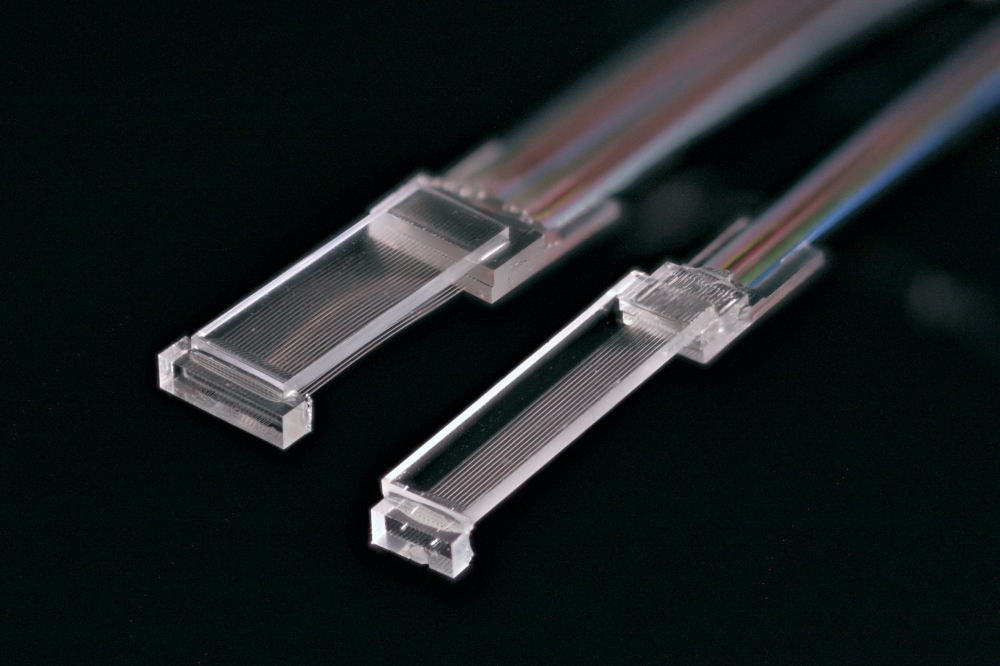
Inspection of fibre arrays (FAU) is critical to ensuring optical coupling interfaces are clean and do not impact PIC testing results
Lensed outputs (on‑chip or attached micro‑lenses) improve coupling but shrink depth of focus and raise angular sensitivity. Contamination near the apex degrades coupling and back‑reflection; the apparent ‘best power’ point can shift with SOP or source linewidth, so stabilized polarization and clean, narrow‑linewidth sources are essential during seek and verify.

Summary
Early planning of the light‑source strategy for CPO‑based PIC testing is critical. The following recommendations can save time and improve yield. If lasers are external (ELSFP), emulate their multi‑channel power, linewidth, and stability characteristics on the test bench. Instrument for scale—expect rising lane counts; prioritise switching, multiport metrology and tight synchronisation. Automate tunability and alignment; deterministic sequencing and fast feedback loops save the most time in production. Bake inspection into the test and treat it as a yield lever. Correlate lab‑to‑line using a modular platform (e.g., MAP‑300) to keep sources, VOAs, switches, and meters on a common control plane and calibration chain for easier change control and faster yield ramp.