Why optical scale-up must be multiplexed
Single-wavelength CPO works for scale-out, but future AI system scale-up demands a fundamentally different architecture built around multi-wavelength slow and wide networks.
By Matt Crowley, CEO, Scintil Photonics
In March 2026, AMD, Broadcom, Meta, Microsoft, NVIDIA, and OpenAI announced a joint consortium to establish an open specification for optical scale-up interconnects. The architecture they aligned on is slow and wide NRZ modulation with wavelength-division multiplexing. When six of the most consequential companies in AI infrastructure publicly agree on the same optical interconnect design for the networks that tie GPUs together into a single scale-up network, then the question of direction is settled.
This announcement definitively settled one of the longest-running debates in datacenter optics: “When will CPO reach the scale-up network?” The next question is no longer whether optical scale-up networks will use wavelength multiplexing, but how fast the industry implements this architecture and how fast it evolves from four wavelengths today to eight, sixteen, and beyond.
Wavelength multiplexing is not a new idea. DWDM was deployed in the telecom industry twenty-five years ago. In principle, the idea is simple: instead of pushing a single channel per fiber, running many channels and scaling bandwidth through multiplexing. Applying this successful optical networking approach to AI scale-up networks is about to reshape AI datacenter architecture the same way DWDM reshaped long-haul telecommunications.
Slow and wide goes fast
The conventional approach to increasing interconnect
bandwidth is brute force: push symbol rates higher, move from simple 2-voltage
NRZ encoding to more complex 4-voltage-level PAM-4 (up to 400Gbps), and carry
more data per fiber. This works in theory, but each step up in modulation bears
a cost. The increased complexity incurs higher latency, power, and costs, as
well as increased heat and space requirements. Single wavelength per fiber
solutions do not scale up the scale.

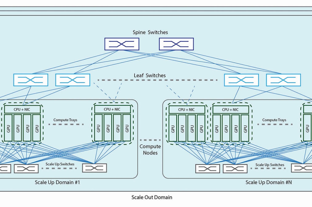
Scale-up
clusters demand ten times the bandwidth of scale-out networks, creating
interconnect bottlenecks only high-speed, dense, and low-power optical can
solve. Source: Scintil Photonics.
Wavelength multiplexing resolves this by scaling bandwidth per fiber through increasing channel count rather than increasing modulation rates. Each wavelength runs at a rate well within NRZ reach, typically 25 to 100 Gbps, depending on bandwidth needs and power budget. At these low rates, the encoding is simple; the signal processing is minimal, and forward error correction can be shallow or eliminated entirely. Aggregate bandwidth scales through multiplication: double the wavelengths, double the bandwidth, without changing the per-channel electronics. The network operator can now choose to run anywhere from 400 Gbps (50 Gbps X 8 ƛ) to 1.6 Tbps (100 Gbps X 16 ƛ), depending on bandwidth needs and power budget.
DWDM scale-up is the architecture NVIDIA described in their published work on a “slow and parallel” interface, A Roadmap Toward Sub-1 pJ/b Optical Interconnect. This landmark paper models a 16-wavelength DWDM microring interconnect and projects a baseline of 3.8 pJ/bit today with a path toward sub-1 pJ/bit through improved receiver sensitivity, integrated optical gain, and more thermally stable rings. It is now the architecture codified by 6 of the industry’s leading companies in the recent OCI MSA specification.
The tail latency tax
Tail latency is the silent killer of GPU cluster economics.
When a thousand GPUs execute a collective operation, they move at the speed of
the slowest processor. A single delayed bit leaves the rest of the cluster to
idle, which hurts utilisation. As cluster size grows from 72 to hundreds, then
thousands of processors, the statistical likelihood of a tail-latency event on
any given operation explodes, as does the risk of an underutilised datacenter.

Example DWDM optical interconnect from NVIDIA’s “A Roadmap Toward Sub 1 pJ/b Optical Interconnect” paper, with an external multi-wavelength light source feeding 16 microring modulators and 16 microring resonators at 100-GHz spacing. Source: NVIDIA.
The slow-and-wide architecture attacks this directly. When per-channel bandwidth is below 100Gbps, NRZ suffices. The processing overhead in terms of time, power, and potential errors diminishes, and latency is reduced and made more deterministic. A low tail latency network is precisely what memory-coherent scale-up domains require for maximum performance and efficiency.
The wavelength staircase: 4 → 8 → 16 → beyond
The consortium’s first-generation specification starts at
four wavelengths based on what is practically possible to make using
traditional laser manufacturing methods. This is a pragmatic beginning. It gets
the ecosystem moving, proves the WDM CPO concept in production of silicon, and
aligns the supply chain for the imminent surge in laser demand. But four
wavelengths at 53.125 Gbps NRZ per channel deliver only 212.5 Gbps per fiber in
each direction. That is meaningful, but it is not yet transformative for multi-rack
scale-up clusters that need multi-terabit links at the package’s edge.

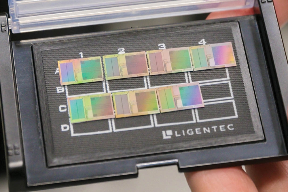
Optical spectrum from a LEAF Light™ single-chip DWDM light
engine showing 16 simultaneous wavelength outputs (F0–F15) at approximately 100
GHz channel spacing, with ±10 GHz wavelength accuracy across all channels.
Source: Scintil Photonics.
The real scaling begins at eight wavelengths. Double the bandwidth per fiber without increasing symbol rate or modulation complexity. At sixteen wavelengths, the architecture unlocks transformative bandwidth for scale-up networks. At this wavelength count, bandwidth density up to 1.6Tbps per fiber at the package edge reaches the regime where fundamentally larger clusters become architecturally feasible without a fiber-count explosion at the package boundary. And the same scaling law continues to thirty-two wavelengths and beyond until network bandwidth and latency are no longer the bottleneck in datacenter performance. Each wavelength increases the capacity on existing fiber infrastructure with no change to the fundamental link design. The per-channel electronics remain the same. The fiber plant remains the same. Only the light source scales.
Future proof your design
For teams designing co-packaged optics today, this trajectory has immediate practical implications. Architectures being laid out now will determine which AI systems can support thousand-GPU cluster configurations in 2028 and beyond. The optimal design is future-proof and can be optimised not only for 4 wavelengths but also beyond. These choices preserve a path to eight and sixteen wavelengths without requiring a major redesign and prevent developers from missing market cycles as wavelength counts jump. An architecture that cannot scale past four wavelengths will need to rework when the specification evolves, and it will evolve, because the physics of scale-up networking demand it.
The scaling law photonics has been waiting for
The semiconductor industry has been through this inflection point twice before.

The LEAF Light™ single-chip DWDM laser source; a
foundry-aligned heterogeneous photonics integration die producing 16
multiplexed wavelengths for co-packaged optics applications. Source: Scintil
Photonics.
Dennard scaling held for three decades: as transistors shrank, power density stayed constant, and each new process node delivered higher clock speeds at no power penalty. That relationship broke down around the 90nm node in the mid-2000s. Leakage currents overwhelmed the voltage scaling that had kept power density in check, and the industry’s free ride on frequency ended. Clock speed plateaued. The industry adapted with multicore architectures, parallelism replacing raw speed.
Moore’s Law continued to pack more transistors onto a chip, but the economic engine underneath it stalled at 28nm. Transistor cost scaling, the 0.7x cost reduction that had compounded with every generation since the 1960s, stopped. Every node since 28nm has been more expensive per transistor, not less. As confirmed by Google at IEDM 2023, cost per transistor is now flat to rising, generation over generation. The industry adapted again, this time with chiplets and heterogeneous integration, assembling systems from specialized dies rather than scaling monolithic chips.
Photonics is arriving at its own inflection, but from the opposite direction. The traditional photonics supply chain has been scaling-limited from the start. Each laser is a discrete device. Each wavelength requires a separate assembly step. Costs scale linearly with channel count because there has been no manufacturing mechanism to bend that curve. This is why, despite decades of investment in silicon photonics, the multi-wavelength laser source has remained the unsolved component: the one piece that could not ride a cost-reduction curve because no such curve existed.
Heterogeneous integration, a fundamental breakthrough in optical manufacturing process technology, changes this equation fundamentally. When III-V gain material is bonded directly onto a silicon photonics wafer in a foundry-aligned process, the laser ceases to be a special-purpose discrete component. It becomes just another circuit element on the die, fabricated, tested, and scaled using the same wafer-level infrastructure that produces millions of photonic devices today. The cost of adding the next wavelength decreases with each process generation, not because the physics change, but because the manufacturing learning curve follows the same pattern as for every other semiconductor-adjacent technology. Importantly, heterogeneous integration not only scales active devices such as lasers, SOAs, and EAMs but also encompasses major photonic circuit elements. This paradigm shift in ultra-integration will allow the photonics industry to finally achieve the scale and design flexibility that enabled CMOS to thrive for decades.
This is what makes wavelength count the relevant scaling law for optical interconnects. Where Dennard scaling gave the industry a free ride on frequency, and Moore’s Law gave it a free ride on transistor cost, wavelength scaling through heterogeneous integration gives photonics its own compounding curve: more bandwidth per fiber, per millimetre of package edge, per microwatt, with each generation improving upon the prior one.
The semiconductor industry learned, both times, that when a scaling law breaks, the replacement is not incremental. It is architectural. Heterogeneous integration is poised to transform photonics from a scaling-limiting technology into a scaling-enabling one. The teams that recognize this transition and design for it now will hold the architectural position when optical scale-up interconnects become the standard configuration for AI infrastructure.
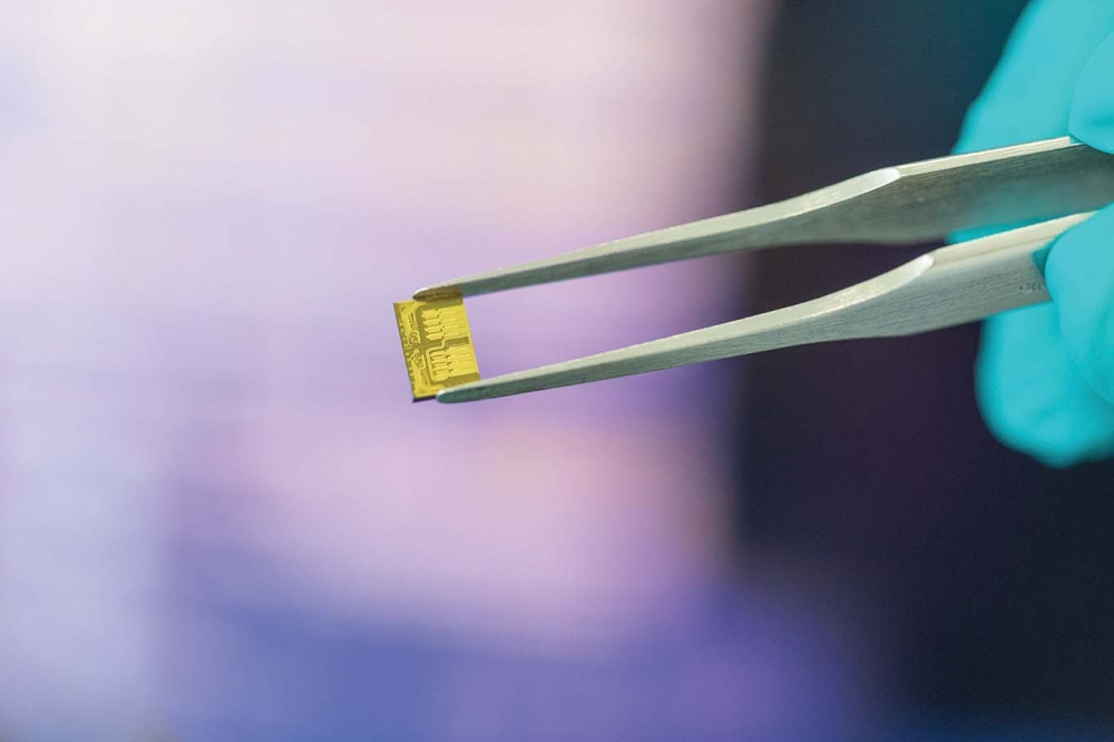
This is the problem we set out to solve at Scintil
Photonics. Our SHIP™ heterogeneous integration technology bonds III-V material
directly onto silicon photonics in a foundry-aligned process flow validated at
Tower Semiconductor. We have already demonstrated our LEAF Light™ single-chip
DWDM laser sources in eight- and sixteen-wavelength configurations compatible
with micro ring-based CPO transceivers. The manufacturing path runs on
established production lines. The cost curve bends with volume. For teams designing
scale-up optical interconnects for what comes after the first generation, that
path is open.