Laser nanoprinting boosts quantum chips

New research argues that femtosecond laser nanoprinting could unlock scalable, room-temperature quantum photonic systems by overcoming manufacturing bottlenecks in photonic integrated circuits.
Photonic integrated circuits are rapidly emerging as the backbone of next-generation quantum technologies.
Still, their path to large-scale deployment has been slowed by manufacturing challenges rather than fundamental physics.
A new perspective by Frank Yao, published in npj Nanophotonics, highlights how fabrication variability, optical losses and the limits of planar chip design are constraining progress toward practical quantum photonic systems.
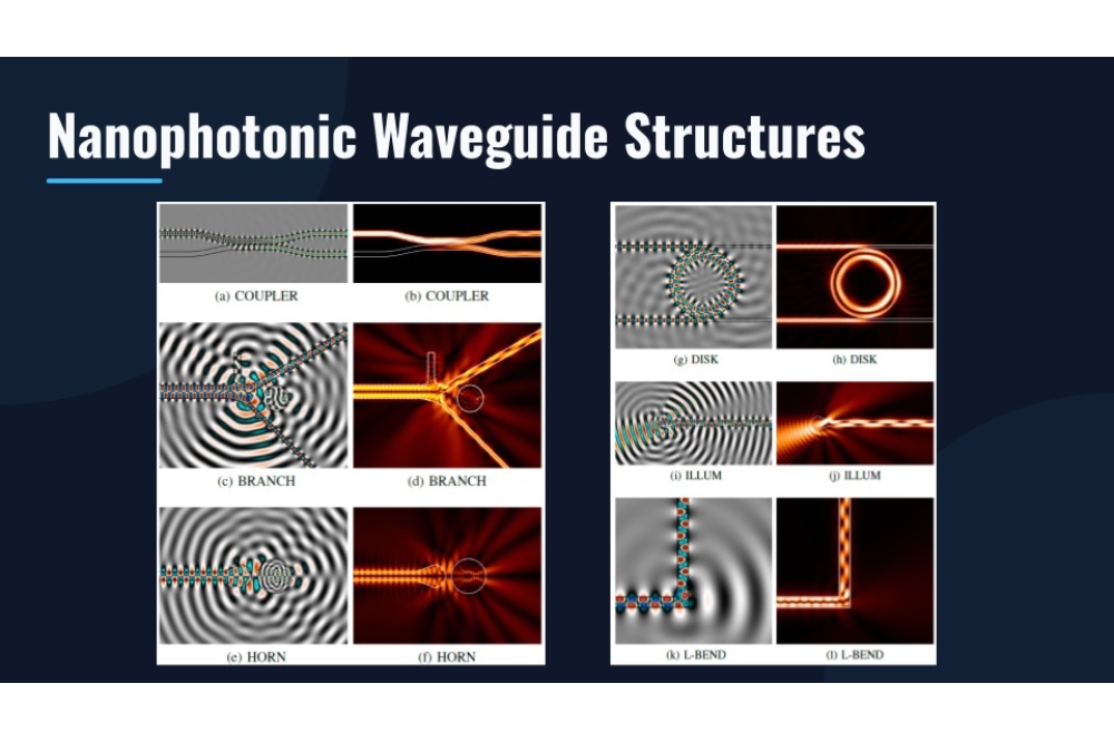
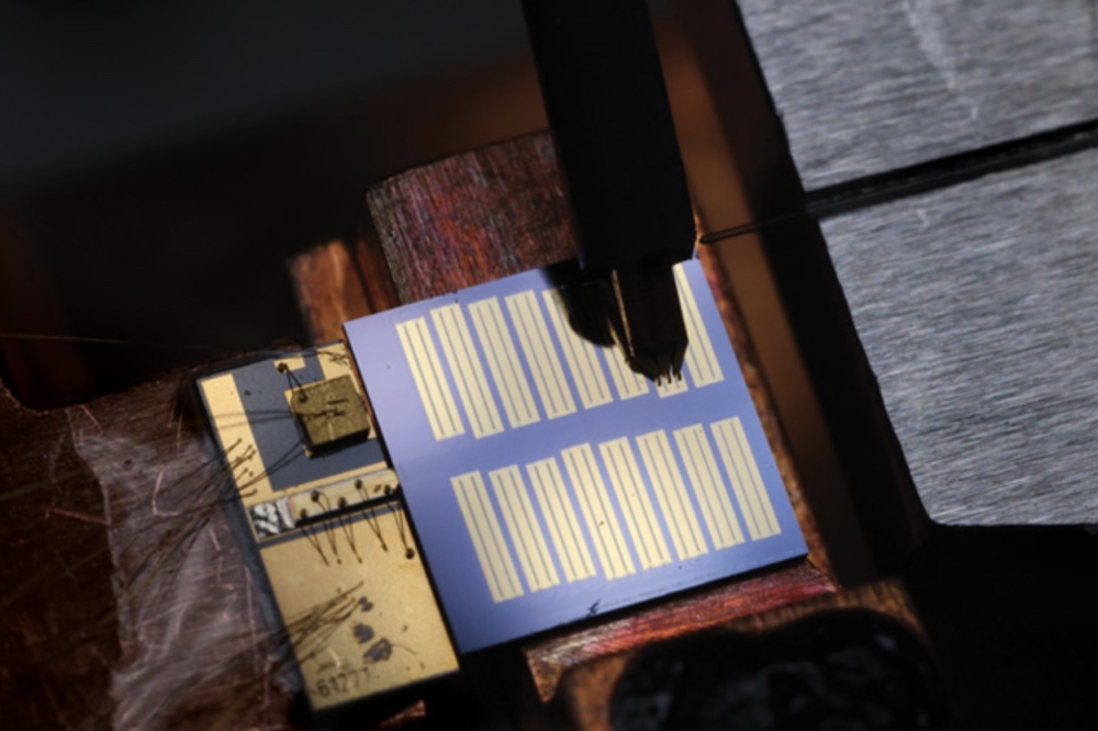
As quantum PICs grow more complex, tiny imperfections at the nanometer scale can introduce phase errors and signal loss, compounding across large circuits and reducing performance.
At the same time, the push toward room-temperature quantum devices—long considered a major milestone for real-world applications—places even tighter demands on stability, integration and packaging.
The paper argues that laser nanoprinting, particularly femtosecond laser direct writing, could provide a crucial solution.
Unlike conventional fabrication methods, this technique enables three-dimensional structuring inside materials, allowing engineers to create photonic interconnects beyond flat chip geometries.
It also offers a way to permanently correct phase errors after fabrication and locally tune optical properties, improving yield and consistency across devices.
These capabilities are especially important as the field moves toward heterogeneous integration, where multiple materials such as silicon nitride, lithium niobate and III–V semiconductors are combined on a single chip.
While such stacks offer the best performance, they also increase fabrication complexity, making post-processing tools like laser nanoprinting increasingly valuable.
The work suggests that integrating laser-based correction directly into photonic manufacturing workflows could shift the industry from laboratory-scale demonstrations to reproducible, scalable production.
This transition is seen as essential for enabling practical quantum technologies, particularly systems that can operate outside cryogenic environments.
While challenges remain, including loss reduction, large-scale process control and standardised testing, the study frames laser nanoprinting as a key enabling layer in the evolution of photonic chips.
If successfully integrated with existing foundry processes, it could accelerate the development of robust, room-temperature quantum photonic systems and help move the field closer to commercial deployment.