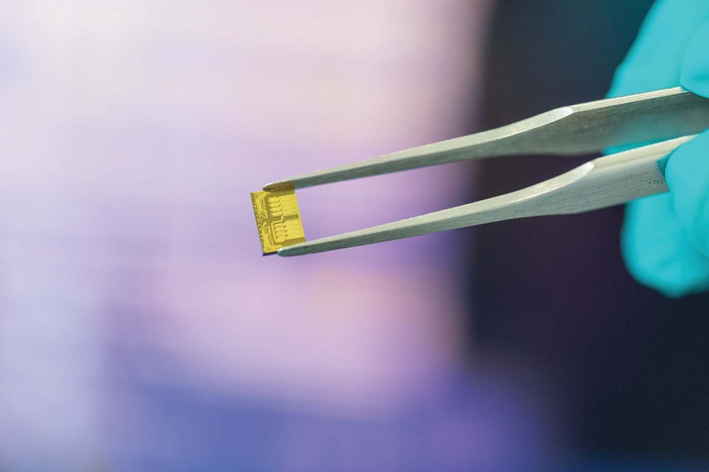
Integrating thin film lithium niobate on low loss PIC platform
Ligentec and UCSD have demonstrated 110 GHz modulators by integrating thin-film lithium niobate with low-loss silicon nitride waveguides on standard silicon wafers, addressing key processing incompatibilities that have previously constrained the scalability of photonic circuits.
by Myriam Labidi, Camiel Op de Beeck, Ligentec
Photonic integrated circuits have progressed from research demonstrations to foundational components of commercial infrastructure. Applications in communications and quantum computing are driving demand for manufacturing platforms that simultaneously deliver high device performance and process scalability.
Lithium niobate offers outstanding electro-optic coefficients for high-speed modulation, while silicon nitride provides ultra-low-loss passive waveguides suitable for complex photonic routing, spot size converters and offers scalability using standard CMOS environment. Monolithic integration of these two materials on a single chip, however, presents substantial fabrication challenges.
The incompatibility is process-level. Stoichiometric SiN waveguides with propagation losses that can achieve below 0.2 dB/m require LPCVD deposition, rendering this thermal budget inaccessible once LN is on the substrate. Additionally, lithium is a forbidden material in CMOS foundries due to its ability to diffuse into, and destroy, transistors on electronic ICs. This inhibits the installation of a monolithic process involving lithium niobate on the majority of today’s semiconductor manufacturing infrastructure.

Material Integration: The temperature challenge
Unlike integration approaches that compromise on material quality, advanced hybrid platforms demand process-level compatibility. Stoichiometric silicon nitride’s exceptional optical performance—propagation losses below 0.2 dB/m depends on high-temperature LPCVD deposition. Lithium niobate, however, begins to degrade above 550 °C, creating a fundamental thermal incompatibility that cannot be resolved within a single sequential process.
Prior approaches using lower-temperature PECVD silicon nitride or reduced film thicknesses compromise the optical and confinement properties that make these materials attractive. The wafer bonding strategy described here resolves this constraint by processing each material independently under its optimal thermal conditions, then combining the two substrates through a low-temperature bonding step that preserves the properties of both.
Prior integration efforts have each involved trade-offs that
limit overall platform performance. Depositing silicon nitride by
plasma-enhanced CVD at reduced temperatures avoids the thermal constraint but
yields films with higher propagation loss than stoichiometric LPCVD material.
Researchers from UC San Diego and LIGENTEC have addressed these constraints through a process-partitioned integration scheme reported in the Journal of Lightwave Technology. Each material is processed under its respective optimal conditions and subsequently bonded at room temperature into a unified platform. The approach yields Mach-Zehnder modulators with 3-dB electro-optic bandwidths up to 110 GHz on standard silicon substrates.
A modular manufacturing strategy
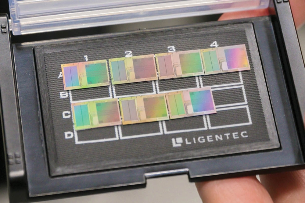
The integration strategy is founded on process partitioning: each material is fabricated under its respective optimal conditions, and the two wafers are subsequently united through low-temperature direct bonding. Realising this approach at wafer scale required addressing a series of challenges, ultimately achieving defect-free bonding across approximately 95% of the wafer area.
LIGENTEC’s proprietary LPCVD process deposits SiN on a 200 mm silicon wafer under optimal thermal conditions. LNOI wafers are prepared in parallel. Contact at room temperature initiates bonding through van der Waals and hydrogen-bond interactions.
The LNOI silicon handle and buried oxide are subsequently removed, leaving the lithium niobate film directly bonded to the underlying silicon nitride structures. Inspection confirms that approximately 95% of the bonded area is free from voids or delamination, a yield consistent with the requirements of volume photonic manufacturing.

The hybrid-mode innovation
A key design consideration in conventional thin-film lithium niobate modulators is the need to etch the LN layer to form ridge waveguides. Although etching provides strong optical confinement, plasma processing damages the crystal structure at the sidewall surfaces, introducing scattering losses and degrading the electro-optic coefficients that determine modulation efficiency. Additionally, etched lithium niobate waveguides often have non-vertical sidewalls, which can lead to unwanted polarisation conversion and mixing.
The present platform avoids lithium niobate etching entirely. Optical mode confinement and routing are determined by the geometry of the silicon nitride waveguides beneath the unpatterned LN film, a configuration referred to here as the hybrid-mode approach. The LN film is left in its as-deposited state, preserving the crystalline quality and electro-optic coefficients of the bonded material.
In passive regions, wider waveguides formed in the SiN layer confine the majority of optical power within the silicon nitride, rendering the overlying lithium niobate slab optically inactive. These waveguides exhibit low propagation loss and support tight bends, enabling compact routing of passive photonic structures.
In active regions, the mode is transitioned vertically through adiabatic tapers. At the end of the transition, approximately 53% of the guided power resides in the LN film, forming the hybrid mode that couples to the applied electric field via the Pockels effect.
Transition loss measured to be a few mdB per taper, a low
value for a vertical inter-layer mode converter. The dual-layer silicon nitride
architecture enables these low-loss transitions while remaining fully
compatible with standard photolithography and dry-etch processing.
Performance that delivers
Mach-Zehnder modulators with phase-shift lengths of 6 mm, 9 mm, and 15 mm were characterised across multiple dies and wafer locations. Key performance metrics showed good uniformity, confirming process consistency at the wafer scale.
The voltage-length product VπL measured 3.8 V·cm. Agreement with predictions based on reported Pockels coefficients for thin-film LN at 1550 nm confirms the bonded film retains its intrinsic electro-optic activity.
The modulator extinction ratio exceeded 35 dB across all devices, indicating well-balanced splitting in both the couplers and the push-pull interferometric arms consistent across multiple dies and wafer locations.
Electro-optic bandwidth measurements yielded the most significant results. The 6 mm modulator achieved a 3-dB electro-optic bandwidth of 110 GHz; the 9 mm and 15 mm devices reached 70 GHz and 20 GHz, respectively. Bandwidth scaled inversely with phase-shift length, as expected for a travelling-wave electrode architecture. These values exceed prior demonstrations of silicon nitride–lithium niobate integration, providing quantitative validation of both the substrate removal strategy and the electrode design.
Looking ahead
This work demonstrates that material incompatibilities, which have historically constrained photonic integration, can be resolved through deliberate process partitioning. By processing each material under its optimal conditions and uniting them via controlled low-temperature wafer bonding, the researchers have established a viable pathway to monolithic platforms that combine best-in-class passive and active components on standard, cost-effective silicon substrates.
The platform’s modular architecture offers clear advantages for commercial development: SiN photonic circuits can be independently designed and qualified using established foundry infrastructure, while LN is incorporated only where active functionality is required. The bonding interface also confers forward compatibility should superior electro-optic materials emerge; they can, in principle, be substituted without redesigning the base SiN platform.
The platform addresses requirements across multiple domains: high-speed coherent transceivers in telecommunications; phased-array antenna remoting and wideband signal processing in RF photonics; and large-scale quantum photonic circuits requiring low propagation loss and precise electro-optic control.
The commercial trajectory for this technology accelerated in January 2026, when LIGENTEC and X-FAB announced an expanded partnership targeting the industrialisation of thin-film lithium niobate integration on both silicon nitride and silicon-on-insulator platforms. The collaboration commits to scaling TFLN-on-SiN and TFLN-on-SOI technologies within X-FAB’s foundry ecosystem using 200 mm wafer processes precisely the manufacturing approach validated by the collaborative demonstration.
“By expanding our partnership with X-FAB, we are giving our customers early access to a broader technology stack that now includes high-volume thin-film lithium niobate integration. This technology enables cutting-edge performance and helps our partners stay at the forefront of innovation in sensing, connectivity and computing applications.” - Thomas Hessler, CEO, LIGENTEC
The partnership establishes a defined pathway from advanced research to industrial-scale production, reinforcing Europe’s position in next-generation photonic integration and signalling broader industry confidence in the wafer-bonding approach.
Continued refinement is already yielding improvements. Long-term reliability testing across temperature and environmental conditions will be essential for qualifying the technology for deployment.
The results presented here confirm that material
incompatibilities previously regarded as fundamental barriers to photonic
integration can be overcome through disciplined process engineering and a
systematic re-evaluation of fabrication sequences. The approach achieves both
the device performance required by next-generation applications and the process
compatibility required for scalable manufacturing outcomes that have
historically been difficult to realise simultaneously on a single integrated
platform.