Electro-optic polymers move from promise to production
As AI data centres push networking to its limits, electro-optic polymers are moving beyond laboratory demonstrations. Advances in reliability, foundry integration and packaging now position them as a production-ready technology for next-generation optical interconnects.
By Robert Blum, Senior Vice President, Sales and Marketing,
Lightwave Logic
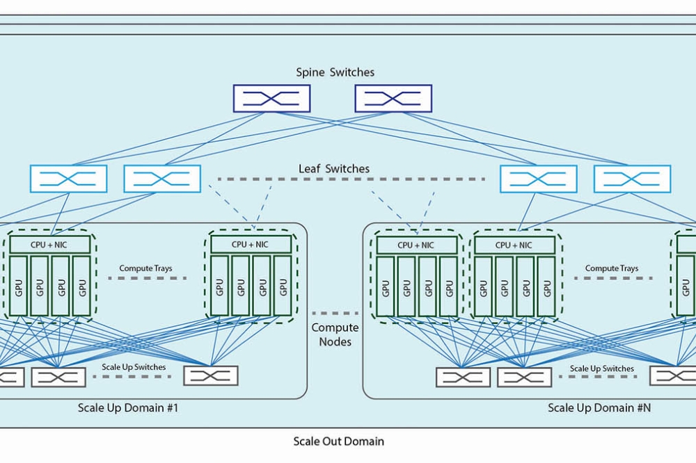
Artificial intelligence continues to drive unprecedented demand for computing, but it is increasingly clear that processing capability alone no longer defines overall system performance. As AI training clusters scale to tens of thousands of GPUs, efficiency depends just as much on how rapidly data can move between processors. In large-scale deployments, the network is no longer a background consideration; it has become a first-order design constraint.
This shift is already reshaping requirements for optical interconnects. Transceivers and the modulators within them must operate at ever higher speeds while consuming less power and occupying smaller footprints. Electrical lane rates are moving from 200 Gbit/s towards 400 Gbit/s, and optical platforms must evolve accordingly. Incremental improvements are proving insufficient. Instead, the industry is being forced to re-evaluate materials and device concepts that can sustain this scaling without imposing unacceptable penalties in power, size, or manufacturability.
Electro-optic (EO) polymers sit squarely in this discussion. Long regarded as an intriguing laboratory technology, they are now being assessed in a much more pragmatic context: whether they can meet the reliability, integration and volume-manufacturing requirements demanded by modern data-centre infrastructure.

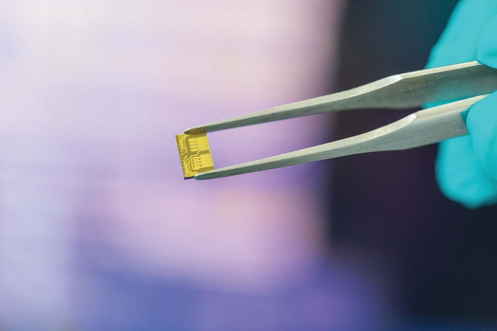
AI data-centre networking bottleneck: As GPU clusters scale, overall system performance increasingly depends on the ability to move data efficiently through optical interconnects, elevating the importance of modulator speed, power and density Schematic of an electro-optic polymer modulator: In an EO polymer modulator, an applied electric field changes the refractive index of the polymer, enabling high-speed optical modulation with low drive voltage
A long history of promise – and scepticism
EO polymers are by no means new. Researchers have explored their use in optical modulators for several decades, drawn by their ability to exhibit large and rapid changes in refractive index under an applied electric field. Unlike many inorganic materials, EO polymers do not rely on the transport of charge carriers to achieve modulation. Instead, their response is dominated by electronic polarisation, enabling extremely fast operation.
Despite these advantages, adoption has historically been limited. The reasons are familiar to anyone who has followed the transition of new materials from laboratory to factory. Questions around long-term stability, sensitivity to temperature, oxygen and humidity, and compatibility with standard semiconductor manufacturing flows all contributed to hesitation. In an industry built on yield, reliability, and repeatability, such caution is not only understandable – it is essential.
However, there is a useful parallel to the evolution of organic light-emitting diodes (OLEDs). OLED materials were once widely viewed as too fragile for mainstream deployment. Their eventual success did not stem from a fundamental change in organic chemistry but from learning how to protect the materials effectively. Encapsulation technologies transformed OLEDs from laboratory curiosities into mass-market products found in smartphones, televisions, and wearables.
EO polymers are now following a similar trajectory.
What makes an electro-optic polymer different?
At the heart of an EO polymer lies a deliberately engineered molecular structure. Dipolar chromophores embedded within a polymer matrix respond directly to an applied electric field by changing the refractive index of the material. Because this process relies primarily on electronic polarisation rather than carrier transport, it can occur extremely quickly, enabling modulation well beyond the limits of conventional semiconductor approaches.
One practical consequence is a very large electro-optic coefficient, typically on the order of several hundred picometres per Volt. In device terms, this allows a substantial optical phase shift to be achieved with drive voltages well below one Volt. For system architects, the implications are straightforward: lower electrical power consumption, simplified driver electronics and compact modulator geometries that help preserve bandwidth density at the chip edge.
At Lightwave Logic, these considerations have guided the development of the Perkinamine electro-optic polymer platform. Rather than optimising for a single headline performance metric, Perkinamine has been engineered with system-level deployment in mind. The polymer matrix exhibits a high glass-transition temperature, enabling compatibility with standard solder-reflow assembly processes. At the same time, the material is designed to integrate cleanly with silicon photonics, complementing a proven high-volume wafer-level manufacturing platform rather than requiring a fundamentally new one.

Integration of EO polymers in a silicon photonics foundry flow: Wafer-level deposition and encapsulation of EO polymers can be incorporated into standard silicon photonics process design kits, supporting scalable manufacturing

Redefining “production readiness”
When engineers talk about production readiness, they rarely mean a single attribute. Readiness emerges from the alignment of several factors: material performance, long-term reliability, process compatibility, and ecosystem integration. For EO polymers, each of these dimensions has advanced significantly in recent years.
Reliability under real operating conditions
Optical modules in data centres operate at elevated temperatures and are expected to function reliably for many years. EO polymers must therefore maintain their electro-optic properties under sustained thermal stress – often around 85 °C – while resisting degradation from environmental exposure.
Advances in molecular design have improved intrinsic stability to the point where projected lifetimes, even at high operating temperatures, extend well beyond typical product requirements. Equally important, the industry now has a much clearer understanding of the dominant failure mechanisms. Experience has shown that exposure to oxygen and moisture, rather than inherent material fragility, drives much of the long-term degradation observed in early devices. Once these mechanisms are understood, effective mitigation becomes possible.
Encapsulation as an enabler, not an afterthought
Encapsulation has emerged as a critical enabler for EO polymer deployment. By surrounding the active material with robust barrier layers, engineers can prevent oxygen and humidity from reaching the polymer, preserving performance over time.
Here, the broader semiconductor industry has provided valuable tools. Over the past decade, thin-film deposition and barrier technologies have matured significantly and are now widely available in foundries. Techniques that were once specialised can be integrated into standard process flows, allowing EO polymer encapsulation to be treated as part of routine manufacturing rather than an exotic add-on. As with OLEDs, production readiness ultimately depends as much on system-level engineering as on the intrinsic properties of the material itself.
Compatibility with silicon photonics manufacturing
Even a reliable material will struggle to gain traction if it requires disruptive processing steps. One of the strengths of modern EO polymer platforms is their compatibility with established fabrication techniques. Deposition processes can closely resemble those used for photoresists, allowing polymers to be applied at the wafer level using familiar equipment.
This compatibility lowers the barrier to adoption. Foundries and device designers can integrate EO polymers into existing silicon photonics flows without re-architecting their manufacturing infrastructure. For an industry that values continuity and predictability, this is a significant advantage.
The importance of the process design kit
In silicon photonics, the process design kit (PDK) plays a central role in translating materials into manufacturable products. A PDK encapsulates the knowledge required to design for volume: process steps, design rules, performance models and verified layouts. Without this framework, even promising technology remains confined to R&D demonstrations.
The emergence of EO polymer PDK modules therefore represents a meaningful inflection point. By defining how materials such as Perkinamine are deposited, encapsulated and integrated alongside silicon photonic components, these kits allow designers to treat EO polymers as part of the standard design toolbox.
At Lightwave Logic, this effort extends beyond material deposition. The PDK also includes guidance on assembly and test, including reference assembly flows for different packaging concepts. This ensures that once a design is proven, customers can transition efficiently towards volume manufacturing rather than encountering new integration challenges at a later stage.
Power and density: why polymers matter now
As data rates climb, power consumption becomes a dominant system-level concern. Every additional milliwatt dissipated by a modulator is multiplied across thousands of links and racks, contributing to cooling challenges and operational cost. Lower drive voltage and reduced power dissipation are therefore not merely attractive features; they are fundamental requirements for scalable AI infrastructure.
EO polymers address this challenge directly. Their high electro-optic coefficient enables efficient modulation with minimal electrical overhead. In parallel, their material properties support compact device geometries, allowing higher bandwidth density at the edges of chips and packages.
What is particularly notable is that this shift is already visible at 200 Gbit/s. At these lane rates, silicon photonics devices enhanced with electro-optic polymers can offer measurable advantages in performance and power efficiency, prompting customers and foundries alike to engage earlier in the design cycle than in previous technology transitions. As a result, evaluation and integration efforts are no longer being deferred until the 400 Gbit/s inflection point.
This density advantage becomes increasingly important as the industry explores advanced packaging concepts such as co-packaged optics. In these architectures, optical interfaces sit in close proximity to GPUs or switches, and space becomes a scarce resource. Smaller, lower-power modulators simplify integration and improve overall system efficiency.
Competing technologies and practical differentiation
Several alternative electro-optic technologies have demonstrated impressive performance and, in some cases, have reached a higher level of maturity in early deployments. However, these approaches often introduce structural challenges as systems move towards volume production. Integration outside standard silicon photonics foundry flows, increased process complexity and reliance on relatively concentrated supply chains all become more significant considerations as lane rates increase and deployment scales.
In this context, electro-optic polymers appear better
aligned with the industry’s long-term direction, where manufacturability,
supply-chain resilience and seamless foundry integration increasingly outweigh
early-mover advantage.
A business model aligned with the ecosystem Another indicator of maturity lies in how EO polymer suppliers engage with the market. Rather than competing directly with transceiver or system vendors, companies such as Lightwave Logic focus on providing materials, intellectual property, and reference designs.
This approach allows partners across the value chain to adopt EO polymers without conflict, accelerating experimentation and deployment. By positioning EO polymers as an enabling technology rather than an end product, suppliers can support a broad range of applications while leveraging the expertise of established device and component manufacturers. This ecosystem-centric model reflects lessons learned across the wider semiconductor industry.
Milestones that signal readiness Scepticism around new materials will not disappear overnight, nor should it. In high-volume manufacturing, confidence is built through qualification data, repeatable processes and multiple independent design cycles.
For EO polymers, the most meaningful signals of maturity include adoption within foundry PDKs, customers progressing through advanced modulator designs, successful completion of industry-standard reliability testing and a clearly defined path to volume wafer processing and packaging. These developments are now beginning to align, shifting the discussion from whether EO polymers can be deployed to when and where they will first see large-scale adoption.
Looking ahead
The demand for bandwidth shows no sign of slowing. If anything, the pace of increase is accelerating as AI workloads continue to scale. Optical technologies must therefore deliver not only the next generation of performance, but a sustainable roadmap beyond it.
EO polymers are increasingly well positioned in this context. Their combination of speed, power efficiency and manufacturability addresses immediate system constraints while leaving room for future growth. Perhaps most importantly, the industry now has the tools, experience and infrastructure required to deploy them reliably at scale.
After many years of development, electro-optic polymers are approaching a practical inflection point. What was once primarily a laboratory technology is now emerging as a production-ready option for next-generation optical interconnects, shaped as much by advances in manufacturing and system design as by materials science itself.