Why scale-up AI networks demand scalable optical test
Scale-up AI networks are pushing optics directly onto switches and AI accelerators. To avoid a manufacturing bottleneck, the industry is shifting optical test from low-parallelism, custom configurations to scalable, automated, IC-style methods.
By Andrew Yick, Senior Director, Product & Test
Engineering, Marvell
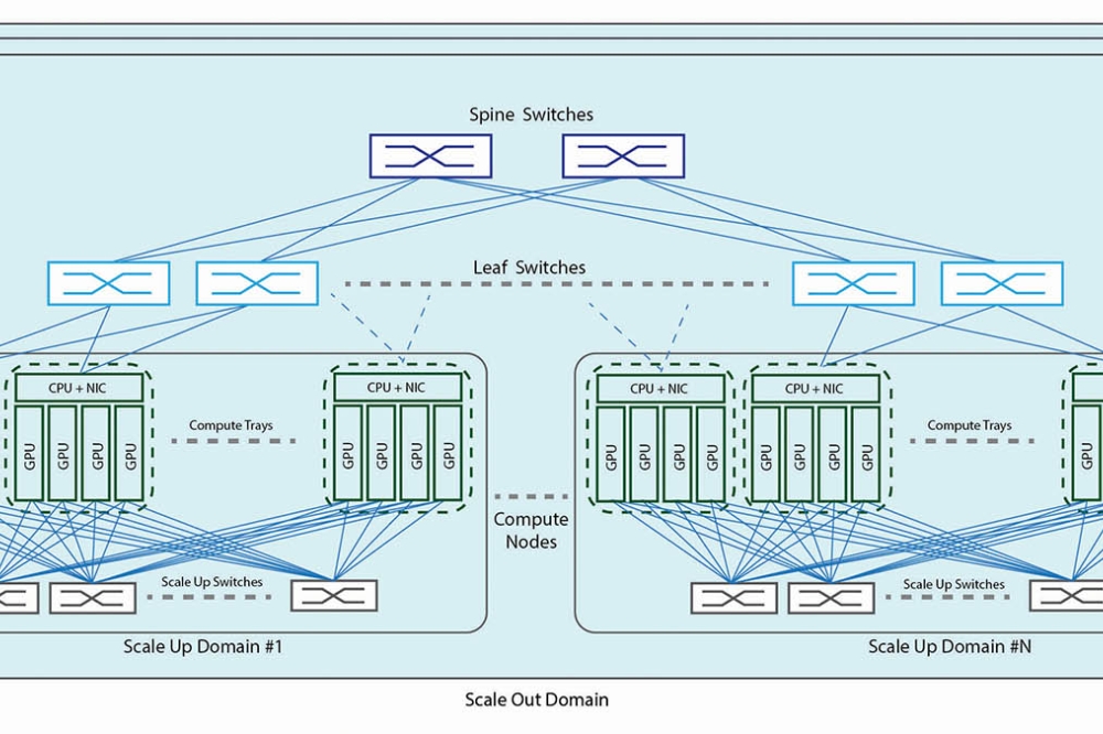
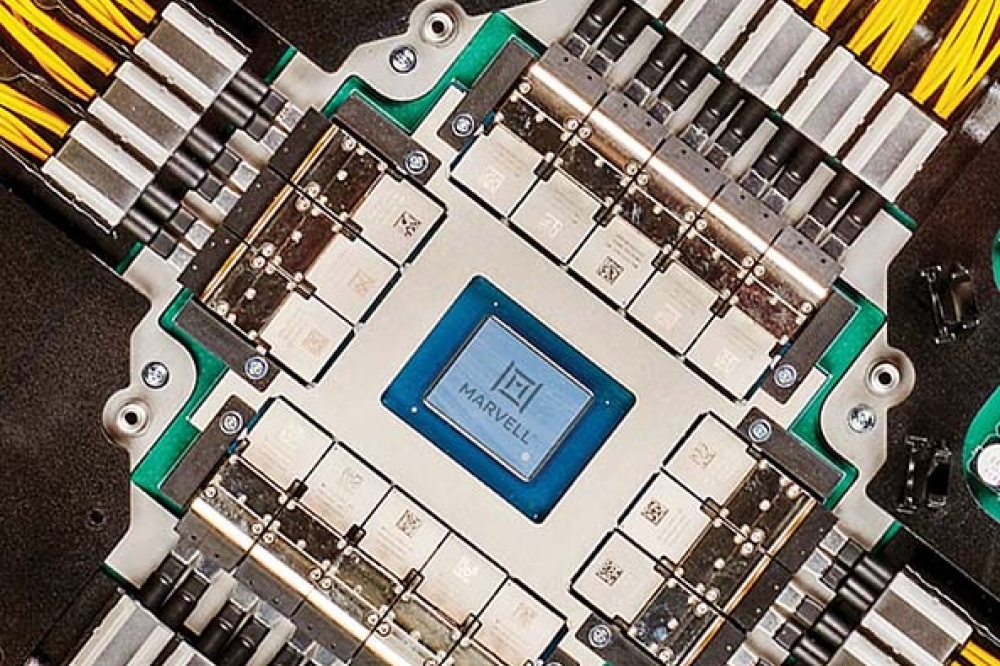
The dominant challenge in modern AI infrastructure is not just the performance of a single accelerator but scaling up to thousands of accelerators (XPUs) in a cluster. Training and inference workloads now depend on an interconnect that can stitch these accelerators into a high-bandwidth, low-latency system, where performance is governed as much by the network as by the compute itself.
As these systems scale, physics asserts itself. Electrical links over copper hit a practical ceiling as routing density and channel loss collide, turning the loss bandwidth product into an impassable constraint. The choice is binary: either move electrical-to-optical conversion closer to the Application-Specific Integrated Circuit (ASIC) or surrender the link budget. Thus, to bypass this electrical wall, optics must migrate from the board edge and onto the ASIC package.
This progression is not an architectural preference; it is a physical necessity. Every serious scale-up roadmap eventually converges on the same outcome: optical interfaces migrating from front-panel modules (including optical-engine-based pluggables) to Near-Packaged Optics (NPO), and ultimately to Co-Packaged Optics (CPO) integrated alongside the compute die. CPO is not the goal in itself, but the inevitable consequence of interconnect bandwidth scaling.
The bottleneck moves to test
Silicon photonics platforms today deliver extraordinary functionality and bandwidth density, but the industry is hitting a manufacturing wall. Historically, optical testing has evolved as a specialized, low-volume practice. Test cells are often custom-built, alignment-heavy, and single-site. Optical instruments typically reside outside the Automated Test Equipment (ATE) ecosystem in rack-and-stack configurations, and throughput is measured in minutes rather than seconds. While these approaches suffice for labs and pilot lines, they break down at high channel counts and production volumes.
The issue is not the measurement rigor, it’s manufacturing
efficiency at scale. As optics move inward toward the ASIC, we still need the
same level of test coverage, but delivered with IC-style parallelism,
repeatability, and automation.
The practical advantage of a mainstream ATE test head is its
high-density instrumentation and native multi-site architecture, allowing one
test program to run across multiple devices in a single touchdown. This
efficiency stems from the ATE’s ability to synchronize complex,
high-parallelism tasks such as coordinating laser sweeps and power meter
captures across all sites simultaneously. To better realize this system-level
coordination at optical wafer test, next-generation opto-electrical probe cards
integrate the optical probe head and on-card fine alignment directly into the
probe card. This integrated architecture allows optical wafer testing to
inherit the semiconductor industry’s high-volume manufacturing model.

Figure 1: Teradyne UltraFLEXplus with Photon 100
single-sided optical wafer probe cell (Courtesy of Teradyne)
Figure 1 illustrates a fully integrated optical test cell
from Teradyne, built around the UltraFLEXplus platform with Photon 100 and a
TEL Precio XL production wafer prober. An integrated opto‑electrical
probe card assembly, auto‑loaded by the prober, brings the
optical probe head to the wafer while maintaining a standard ATE test flow.
Electrical instrumentation resides natively inside the tester, while the
optical sources and measurement resources are consolidated in an external rack
that is fully interfaced and safety interlocked to the test head. Optical
connections are then blind-mated through a standard load board at the prober
docking interface.

Figure 2: Technoprobe integrated opto-electrical probe card
for high-volume production (Courtesy of Technoprobe)
Figure 2 highlights a Technoprobe integrated opto-electrical probe card architecture. First-generation integration using static optics with expanded-mode interfaces is already deployed in volume production today, with solutions available from vendors such as Jenoptik. The figure shows the next-generation evolution: cards with integrated piezos for sub-micron fine alignment.
The solution also integrates a native on-card controller and a local high-voltage step-up to drive the piezos, avoiding the need for high-voltage sources from the tester. By combining the prober’s coarse positioning with local high-speed alignment at the device interface, this Outsourced Semiconductor Assembly and Test (OSAT)-friendly architecture eliminates bulky optomechanics, effectively closing the gap between lab-grade precision and factory-friendly volume.
Shift left or absorb the cost
As optical functions are integrated into multi-chip modules (MCM), the full-rate optical behavior may only be uncovered once the CPO-Integrated XPU package is fully assembled – after substantially more silicon value has already been added and when rework may be limited or unavailable.
Optical devices are no longer pluggable modules; they are
built into engines and chiplets, co-packaged alongside ASICs, memory, and
substrates. At this level of integration, a single failing optical channel can
force the scrap of an entire high-value assembly.
Late discovery is therefore economically untenable. The only
viable strategy is to shift meaningful optical test earlier in the
manufacturing flow, specifically to the wafer level, but only if those early
measurements are predictive and correlated to full-rate performance in the
final assembly. This logic is familiar to semiconductor manufacturing, but its
implications are more severe for integrated optics because the financial
penalty for a late-stage failure is so high. Establishing Known-Good-X (KGx) is
no longer optional: where “X” is the unit being certified as known good – die,
optical engine, or chiplet – before it is integrated into a higher-value
assembly.

Figure 3: “Shift-left” optical test improves manufacturing
economics by reducing scrap exposure and maximizing throughput
Figure 3 illustrates the direct impact of test timing on
manufacturing economics. As devices move through the assembly process, defect
discovery becomes disproportionately expensive, making “shift-left” testing a
fundamental requirement for scalable manufacturing economics. This strategy
prioritizes short cycle-time highly parallel tests at the wafer level, in
contrast to the long cycle-time and capital-intensive tests required once
optics are integrated into a full CPO-Integrated XPU module.
A unified optical test insertion framework
Scaling optical test requires a structured framework with
explicit test insertions, providing a common language across design, test, and
manufacturing. Figure 4 illustrates this hierarchy:
- Insertion 1 (Photonic IC Wafer): The PIC wafer is screened using electrical and optical parametric measurements to establish Known Good Die (KGD) at the earliest possible stage. This initial gate employs high-parallelism optical scans to generate a parametric map of the wafer, which may include critical spectral characterization, modulator efficiency, and polarization-dependent loss (PDL) measurements. By identifying marginal components early, the exponential cost of integrating defective silicon into high-value downstream assemblies is avoided.
- Insertion 2 (PIC + EIC): This occurs once the photonic and electronic ICs are bonded, representing the first stage of multi-die integration. Electro-optic transfer characteristics may be measured at speed and correlated back to initial wafer-level results (e.g., modulation response, eye quality, and other high-speed figures of merit). This correlation ensures that the bonding or die-attach process has not degraded the PIC’s performance, while also assessing the health of the inter-die connectivity.
- Insertion 3 (Optical Engine): Engines or chiplets undergo final calibration and functional testing after fiber attach or connectorization. These tests establish KGx status for the assembly, serving as the final gate to prevent defective units from propagating into multi-chip modules. Validation at this stage typically expands to include link-budget verification and thermal characterization to ensure that fiber-to-chip coupling remains stable across the full operating temperature range.
While the final test insertions, including the CPO XPU and system-level assemblies, are likewise critical, their primary role shifts to validating overall functionality. The final test insertions are not where component-level yield problems should be discovered. By shifting the burden of discovery to early PIC-centric insertions, this structured approach ensures that yield is managed at the most cost-effective stages of the production flow.

Figure 4: Optical test insertion hierarchy for scaling
photonics test from wafer screening to system-level
Industrializing the optical test methodology
The transition from treating optics as a specialty test to
an IC-style methodology is already underway. This philosophy now extends beyond
the wafer to the chiplet level (Insertion 3), where the challenge shifts to
verifying integrated assemblies.

Figure 5:
Chiplet-level optical test cell combining an Advantest V93000 EXA direct-dock
test head with an MPI DTS650-DI prober with integrated optical alignment
(Courtesy of Advantest and MPI)
Figure 5 illustrates a chiplet-level optical test cell built around an Advantest V93000 EXA and an MPI DTS650-DI chip-level prober. In this configuration, the optical alignment function is integrated into the prober itself, enabling bottom-side or edge coupling of the optical chiplet within a standard OSAT-style manufacturing footprint. This removes the external opto-mechanics that typically obstruct direct-dock operation and complicate automation. Crucially, the tester remains on a standard ATE platform with a conventional load board and docking interface. Electrical resources reside natively in the test head, while optical resources reside in a dedicated test cabinet and are routed into the cell under full tester control. The result is a manufacturing-ready system in which optical chiplets can be handled, aligned, and verified alongside digital content without resorting to custom bench setups.
These proof points change the conversation. The question is
no longer whether a scalable optical test is possible, but how quickly the
ecosystem can standardize around it. To reach a true global scale, several
pieces must still fall into place:
- Native ATE Instrumentation: We require native optical instrumentation that resides directly inside the ATE test head, reducing the reliance on external optical racks either adjacent to or bolted onto the test cell.
- Defined Standards: The ecosystem requires industry-wide agreement on standards for scale-up optical networking—including wavelengths, fiber counts, modulation formats, and target power levels as well as unified calibration and correlation methods.
- Physical Interfaces: Standardized physical interfaces, such as common PIC port definition, detachable connector solutions, and blind-mate docking, are essential for manufacturing adoption.
Accelerating the adoption of these standards will determine how quickly “optics as an IC” moves from a custom, low-volume specialty test to a mainstream manufacturing reality.
Design-for-test: the shared responsibility
As optics matures into an IC-style manufacturing problem, design and test must converge earlier in the product cycle. Scalable optical test cannot be retrofitted as a final stage of development; it must be explicitly enabled by design. Optical Design-for-Test (DfT) is therefore no longer a luxury, but a requirement.
Specific architectural features determine whether a device
can be economically tested at scale:
- Access Points: Specific points for parametric measurement must be integrated into the design. These access points may include dedicated optical DfT paths and integrated monitor diodes that allow for in situ structural checks.
- Correlation Support: Built-in support is needed to correlate data across various test insertions. By burning unique IDs and calibration trims during wafer-level screening, a digital imprint is created that ensures parametric traceability in downstream test insertions.
- Parallel Test Strategies: Parallel testing is essential for high-volume throughput—maximizing tester-resource utilization and enabling multi-site operation. Supporting simultaneous tuning and calibration of all transmitter/receiver channels, without compromising measurement integrity, is key to meeting AI-scale takt times. Built-In Self-Test (BIST) further enables this parallelism by generating at-speed stimuli and leveraging loopbacks to screen channels in situ, reducing dependence on external optical instrumentation.
Without these front-end considerations, even the most advanced ATE infrastructure will struggle to maintain yield, test coverage, and cycle-time targets.
For the test community, the implication is clear: the industry must move away from the legacy optical module era practices in favor of integrated, automated solutions that leverage existing semiconductor infrastructure.
Optics as a first-class manufacturing domain
Scale-up AI networks depend on optics, and optics, in turn, now depends on test. What began as a specialized, lab-centric practice must now mature into a first-class manufacturing capability, aligned with the rigorous methods that have sustained semiconductor scaling for decades.
This transition requires deep collaboration
across design, test, instrumentation, and manufacturing, and
it is already well underway across the ecosystem. As scale-up AI clusters
advance, optics must follow the same DfT, shift-left, and ATE-enabled
manufacturability playbook that has long governed high-volume electronics. The
mantra for the upcoming years is simple: If it cannot be tested like an IC, it
will not scale like one.