Reimagining electromagnetic simulation for photonics
A new approach to electromagnetic simulation is unlocking speed, accuracy, and scalability in photonics.
Electromagnetic simulation sits at the heart of photonic device innovation, but many of today’s tools are built on decades-old methodologies that were never designed for modern hardware demands. As applications such as co-packaged optics and AI-driven infrastructure accelerate, the need for faster, more accurate, and more scalable simulation has become critical.
In this conversation, Sarab Chopra, Editor at PIC Magazine, speaks with Luke Voss, Chief Product Officer at EMTR, about how EMTR is redefining simulation for photonics, the limitations of legacy approaches, and what this shift means for the future of silicon photonics and PIC design.
SC: What makes EMTR fundamentally different from existing electromagnetic simulation tools used in photonics?
LV: EMTR represents a decade-long effort to rethink what electromagnetic simulation should look like on modern computing hardware. Traditional tools—particularly those based on Finite-Difference Time-Domain (FDTD) methods—trace their origins back to the 1980s, both in algorithm design and hardware assumptions.
Today, those legacy approaches are hitting practical limits. It’s not uncommon for companies to require over a terabyte of memory just to simulate a simple two-element photonic device. That’s clearly not scalable.
EMTR changes that equation entirely—we can solve the same problem using just a few gigabytes of memory on a standard laptop. That’s the kind of shift needed to keep pace with modern photonics design.
SC: How do your algorithms improve simulation speed and accuracy for PIC and silicon nanophotonics design?
LV: The performance gains come down to two key advantages: dramatically reduced memory requirements and highly repeatable accuracy.
First, EMTR is built on boundary integral equations and Green’s Function methods. Instead of modeling the entire 3D volume like FDTD solvers, we reduce the problem to surfaces. So rather than a million-point 3D mesh, we’re working with something closer to ten thousand points. That reduction scales even better as problems grow larger.
Second, we use spectral methods, which are extremely efficient in terms of accuracy. With conventional methods, doubling mesh density might improve accuracy by a factor of two to four. With spectral methods, that improvement can be orders of magnitude higher.
In practical terms, EMTR can achieve four digits of accuracy using just 16 points per wavelength—something that traditional solvers would struggle to match even with much finer meshes.
SC: What specific challenges in photonic device development does EMTR aim to solve?
LV: At its core, EMTR enables faster, more accurate, and more reliable simulations across a wide range of photonic components.
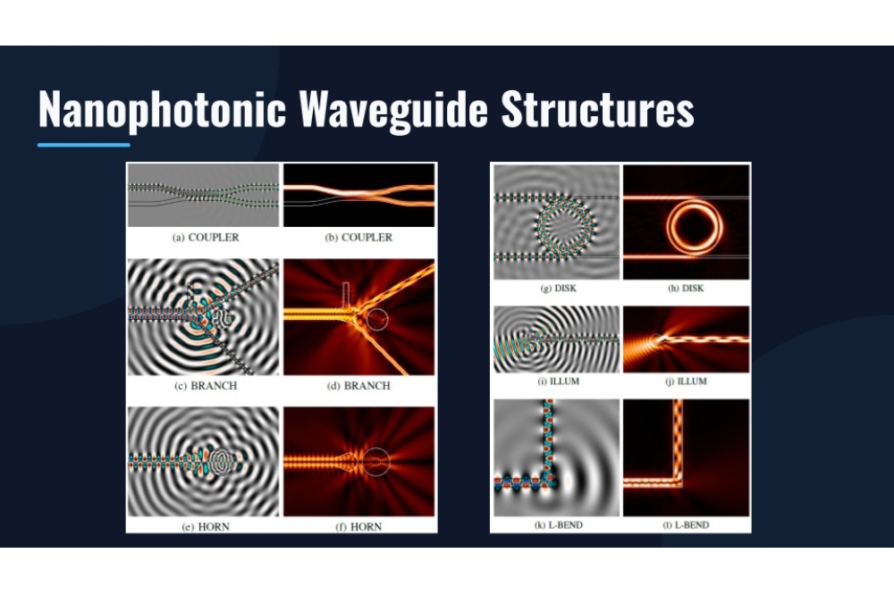
This includes everything from fiber-to-chip interfaces like grating and edge couplers, to signal-processing elements like ring resonators, to more advanced structures like metasurfaces and complex photonic “black box” systems.
What’s important is accessibility. Problems that previously required large-scale cloud computing can now be handled on a laptop or workstation. At the same time, EMTR opens the door to modeling large, multi-component systems that were simply out of reach before.
That’s especially critical for inverse design workflows, where rapid iteration depends on both speed and accuracy.
SC: How do you see simulation shaping the next generation of silicon photonics and PIC innovation?
LV: We’re seeing massive investment flow into silicon photonics, and that’s only accelerating. One major trend is co-packaged optics—bringing photonics closer to GPUs to support AI workloads.
As devices become more compact and complex, you’re packing more functionality into smaller spaces. That introduces risks like unintended electromagnetic coupling between components.
Simulation becomes essential in this context. EMTR allows designers to model these dense, highly coupled systems accurately, optimize designs to take advantage of those interactions, and significantly reduce the number of fabrication and testing cycles needed to reach a working device.
Ultimately, simulation is becoming a central driver of innovation—not just a validation step.
SC: Who are the primary users of EMTR within the photonics ecosystem?
LV: Our users span the full ecosystem.
That includes PIC designers doing day-to-day engineering work, researchers pushing the boundaries of photonic components, and fabrication facilities looking to develop more robust and manufacturable process design kits (PDKs).
Each group benefits from faster, more accurate simulations that integrate into their existing workflows.
SC: What are your next steps for expanding EMTR’s capabilities in photonics design?
LV: Our immediate focus is deep engagement with the market—understanding the real challenges teams face in photonics product development.
We’re continuing to refine our solver while building out capabilities that support inverse design workflows and component libraries, especially for PDK developers. Metamaterials are another key area where we’re actively gathering insights to better support emerging use cases.
Beyond product development, we’re also prioritising partnerships and broader ecosystem engagement. The goal is to deliver a flexible, high-performance solution that keeps evolving alongside the industry.