Integrated photonics confronts testing, packaging and scale

As photonic integrated circuits move toward larger-scale
deployment in AI systems, communications and sensing, the industry is
increasingly confronting the practical challenges of testing, integration and
manufacturability. Discussions at PIC International 2026 highlighted how these
pressures are reshaping optical metrology, packaging strategies and
next-generation photonic architectures.
By Sarab Chopra, Editor, PIC Magazine
While photonic integrated circuits continue to advance in capability and complexity, speakers at this year’s PIC International made it clear that the industry’s next challenge lies not simply in improving device performance, but in understanding how to test, integrate and manufacture these systems at scale.
Across the conference, attention increasingly focused on the growing disconnect between the rapid evolution of PIC architectures and the ability of existing testing and packaging strategies to keep pace.
As photonic devices incorporate larger numbers of optical functions, operate closer to physical limits and move into new application spaces, conventional approaches to characterization are becoming increasingly inadequate.
At the same time, the application landscape for integrated photonics is expanding rapidly. Alongside the continuing growth of silicon photonics for communications and AI infrastructure, researchers are now exploring nonlinear photonic platforms capable of extending integrated photonics deep into the ultraviolet.
Presentations during PIC International 2026 examined many aspects of this transition, including the challenges of high-volume PIC testing, the impact of co-packaged optics on optical metrology, and the development of aluminium nitride photonic circuits for far-ultraviolet light generation.
What became increasingly clear throughout the event is that the PIC industry is moving beyond the phase where success is measured primarily by demonstrating isolated device functionality. Instead, the sector is now confronting the realities of scaling integrated photonics into manufacturable technologies that can satisfy the reliability, cost and performance requirements of communications, AI infrastructure, sensing and emerging quantum systems.
In many respects, integrated photonics is beginning to encounter challenges that mirror those faced by the semiconductor industry decades earlier. As circuits become denser and functionality becomes increasingly interconnected, the difficulty of understanding system behaviour rises sharply. Tiny process variations can alter performance, thermal effects become more difficult to manage, and packaging increasingly influences overall device characteristics.
At the same time, expectations placed on photonic systems continue to rise. AI-driven data centres require dramatically higher bandwidths and lower power consumption, sensing applications demand greater precision and stability, and new nonlinear photonic platforms are pushing integrated optics into spectral regions that were previously inaccessible.
Against this backdrop, several presentations at PIC International suggested that the future competitiveness of the sector may depend less on isolated breakthroughs in device physics, and more on the industry’s ability to build robust ecosystems around testing, packaging, automation and integration.
Testing under pressure
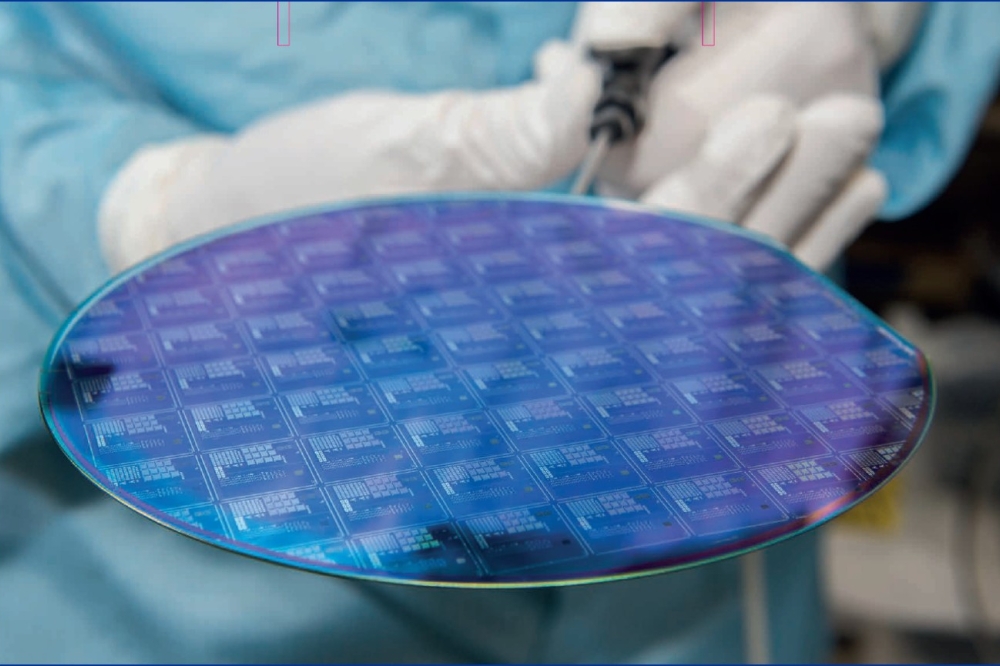
Photonic integrated circuits promise many compelling advantages over discrete optical systems. They enable compact, multifunctional architectures with high-density integration, wafer-scale fabrication and increasingly sophisticated electro-optic functionality.
But according to Marc-André L’Aliberté, Marketing Director at APEX Technologies, these same advantages are also creating major challenges for optical characterization and production testing.
Speaking at PIC International, L’Aliberté explained that PIC functions are highly interdependent, making observability increasingly difficult.
“Functions cannot be isolated, effects are coupled, and one variable can create multiple impacts,” he remarked, while noting that modern PICs operate increasingly close to physical performance limits.
This complexity is amplified by wafer-scale manufacturing, where small process variations can generate significant device-to-device performance differences. Thermal sensitivity, power fluctuations and packaging constraints further complicate characterization.
According to L’Aliberté, the challenge is not that the required measurements are new. Engineers still need to measure insertion loss, return loss, linewidth, chromatic dispersion, polarization effects and phase behaviour, all familiar quantities within photonics.
What has changed is the level of performance now required.
“Measurements are not new, but now devices operate closer to physical limits,” he explained.
One consequence is that no single measurement technique can provide a complete understanding of PIC behaviour.

For spectral analysis, grating-based optical spectrum analysers offer measurement speeds five-to-ten times faster than interferometric systems. However, interferometric approaches deliver dramatically higher resolution, reaching approximately 5 MHz and enabling the observation of side modes and comb lines.
Similarly, power and loss measurements involve trade-offs between spectral and spatial information. Tunable laser and power-meter systems provide fast, cost-effective insertion-loss measurements, while optical frequency-domain reflectometry offers high spatial resolution and distributed backscattering analysis.
Polarization characterization introduces further complications. Depending on the application, engineers may prioritise speed, sensitivity, spectral coverage or measurement accuracy. As a result, testing increasingly relies on combinations of polarimeters, polarization state generators, polarization scramblers and optical vector analysers.
L’Aliberté argued that future PIC testing will depend heavily on integrating complementary measurement techniques into unified automated architectures.

“A complete testing solution requires application-specific tests combined and automated,” he explained, highlighting the growing importance of synchronized instrumentation, thermal control, probe stations and automated handling.
He also distinguished between the priorities of research laboratories and manufacturing lines.
In research environments, engineers require highly versatile systems capable of exhaustive characterization and benchmarking. Production environments, by contrast, prioritise speed, robustness and scalable test strategies.
The emerging approach, according to L’Aliberté, is to first characterise the full parameter space during development, before reducing the test set through correlation and optimisation for production deployment.
That transition from exhaustive laboratory characterisation to streamlined production testing is becoming one of the defining engineering challenges for integrated photonics.
Historically, many photonic devices were produced in relatively modest volumes, allowing engineers to tolerate lengthy and highly specialised measurement procedures. But the emergence of silicon photonics for datacentres, co-packaged optics and sensing is rapidly changing those economics.
Wafer-scale manufacturing now demands test methodologies capable of operating at high throughput while maintaining increasingly stringent performance tolerances. This creates an inherent tension between measurement depth and manufacturing efficiency.
As one speaker noted during discussions at the conference, every additional measurement improves understanding of the device, but also increases testing time, equipment complexity and production cost.
For highly integrated PICs, the problem becomes especially acute because optical functions are no longer isolated building blocks. Losses, polarization effects, phase shifts and thermal interactions often influence one another simultaneously, making simplified testing strategies difficult to implement.
The growing importance of statistical process control also featured prominently in conversations around the conference. Rather than relying solely on pass-fail testing, manufacturers increasingly need large datasets capable of revealing subtle process drifts before yields begin to deteriorate.
This trend is likely to accelerate as PICs become larger and more heterogeneous, incorporating lasers, modulators, detectors and electronic control functions onto common platforms.
Co-packaged optics and the scaling problem
Another major theme at PIC International concerned the rapid emergence of co-packaged optics for AI and high-performance computing infrastructure.
Matthew Adams, Director of Product Management at VIAVI Solutions, explained how the integration of silicon-photonics engines directly beside switch ASICs is reshaping optical test requirements.
“Co-packaged optics is rapidly reshaping next-generation switch architectures,” said Adams.
The attraction of CPO is clear. By moving optics closer to the switching silicon, system designers can significantly improve bandwidth density and power efficiency, both critical metrics for AI data centres.
However, this tighter integration substantially complicates optical testing.
According to Adams, PIC test architectures must now adapt to three major trends: higher levels of functional integration; the use of external continuous-wave laser sources; and dramatic increases in lane counts.
Compared with conventional pluggable optics, co-packaged systems involve far more optical fibres per device under test. At the same time, testing increasingly shifts toward wafer- and die-level qualification.
“PIC yields drive parametric testing,” explained Adams.
Unlike pluggable modules, where much of the functionality is self-contained, co-packaged architectures require external digital and optical sources during testing.
As lane counts scale from 400G towards 1.6T and beyond, testing throughput is becoming a major bottleneck.

“Test times scale with the number of paths,” warned Adams, while noting that yield pressures are simultaneously driving tighter performance tolerances.
To address these challenges, the presentation examined modular metrology solutions spanning waveguide characterization, parametric testing and functional system validation.
Early-stage testing of silicon microrings employs swept-wavelength and polarization-sensitive measurements, while larger functional test systems support increasingly complex multi-lane architectures.
The growing importance of external optical injection sources for CPO testing was also highlighted. These sources require high output powers to overcome splitter losses, narrow linewidths to accurately characterise modulators, and high polarization extinction ratios.
One example discussed during the presentation delivered more than 24 dBm optical power with instantaneous linewidths as low as 33 kHz.
Packaging and connector integrity are becoming equally critical. The rise of co-packaged optics represents one of the clearest examples of how integration is fundamentally altering the photonics landscape.
For many years, pluggable optical modules provided a relatively clean separation between optics and electronics. Optical transceivers could be independently developed, tested and replaced, while electrical switching hardware evolved on a separate trajectory.
Co-packaged optics disrupts that model by moving optical engines directly beside high-performance switch ASICs. This shortens electrical interconnect distances and improves energy efficiency, but it also tightly couples optical and electronic design constraints.
As a result, optical testing increasingly becomes intertwined with system-level validation.
Instead of evaluating isolated optical modules, engineers must now characterise highly interconnected systems involving optical, electronic and thermal interactions simultaneously. This significantly complicates manufacturing workflows.
The increase in fibre density also presents substantial practical challenges. Large lane counts require highly parallel optical interfaces, tighter alignment tolerances and more sophisticated automated handling systems.
Even connector cleanliness becomes more critical as fibre counts increase. Small particles or scratches that might once have affected a single channel can now compromise much larger portions of the system.
Several presentations during the conference suggested that automation will become essential for managing this complexity. Automated inspection, alignment and synchronization are increasingly moving from desirable features to operational necessities.
At the same time, external laser sources are becoming more important within co-packaged optical architectures.
Unlike many traditional pluggable systems, some co-packaged approaches distribute optical power externally, placing greater demands on linewidth stability, polarization control and optical power management.
This shift is influencing the design of optical test equipment itself. Test platforms increasingly require modularity, high port counts and the ability to support multiple insertion points throughout the manufacturing flow.
Beyond datacentres, many delegates also viewed co-packaged optics as part of a broader movement toward tighter photonic-electronic integration across the industry.
Whether in AI hardware, sensing systems or future quantum technologies, the ability to combine optics and electronics more closely is widely seen as essential for improving system efficiency and reducing interconnect bottlenecks.
Nonlinear photonics moves into the ultraviolet
As photonic systems move toward increasingly dense fibre-array interfaces, automated inspection and cleaning systems are becoming essential for identifying scratches, particulates and mobile contamination on connectors.
While many presentations focused on communications and AI infrastructure, another talk highlighted the expansion of integrated photonics into entirely new wavelength domains.
Scott Burroughs of Uviquity presented progress in aluminium nitride photonic integrated circuits designed for nonlinear frequency conversion into the far-ultraviolet spectrum.
The work targets wavelengths around 222 nm, a region attracting significant interest because of its ability to inactivate pathogens while remaining safe for human skin and eyes.
Potential applications extend beyond disinfection to semiconductor inspection, environmental sensing, defence technologies and advanced photonics.
According to Burroughs, researchers have now demonstrated the generation of 222 nm far-UVC light on a scalable aluminium nitride photonic platform.

The approach relies on second-harmonic generation, in which photons from an integrated blue laser source are frequency-doubled within nonlinear AlN waveguides.
Efficient second-harmonic generation depends critically on phase matching, ensuring that generated harmonic waves remain constructively aligned during propagation.
Burroughs reviewed several phase-matching techniques, including quasi-phase matching, birefringent phase matching and modal phase matching.
Aluminium nitride is particularly attractive for this application. The material combines a wide 6.2 eV bandgap with transparency spanning approximately 0.2 μm to 5.5 μm, strong second-order nonlinearity and compatibility with scalable III-nitride semiconductor processing.
Researchers have already demonstrated low-loss AlN-on-sapphire material grown by MOCVD, with intrinsic losses measured at approximately 2.7 dB/cm at 447 nm.

Fabrication employs standard e-beam lithography and chlorine-based dry etching to define waveguides.
Using this platform, second-harmonic generation spanning wavelengths from 214 nm to 300 nm has now been demonstrated.
According to Burroughs, multiple generations of samples representing thousands of devices and measurements have been produced.
The presentation also discussed a compact hybrid photonic package integrating a commercial blue laser diode with an AlN frequency-conversion chip.
Future work will focus on reducing waveguide losses, enhancing nonlinear coefficients using scandium-doped AlN structures, and pursuing heterogeneous integration of GaN laser sources directly onto the PIC platform.
Although much of the conference focused on communications and AI infrastructure, the work on aluminium nitride also illustrated how integrated photonics is steadily broadening beyond its traditional application areas.
Historically, many PIC platforms have concentrated on infrared wavelengths relevant to fibre-optic communications. Extending integrated photonics into the ultraviolet introduces an entirely different set of material and fabrication challenges.
Optical losses generally rise sharply at shorter wavelengths, fabrication tolerances become tighter, and suitable nonlinear materials are limited. Generating far-UVC light on-chip therefore represents a significant technical milestone.
The attraction of the 222 nm spectral region is considerable. Unlike conventional germicidal UV sources, far-UVC light appears capable of efficiently inactivating pathogens while remaining safe for occupied environments.
This has generated growing interest in applications ranging from hospitals and public transport systems to clean manufacturing environments.
At the same time, ultraviolet integrated photonics may ultimately find roles in spectroscopy, semiconductor metrology, environmental monitoring and advanced sensing.
One particularly notable aspect of the presentation was the emphasis on scalability.
Rather than demonstrating a laboratory-scale optical experiment, the work focused on creating a semiconductor-compatible photonic platform capable of supporting large numbers of devices and future packaging integration.
That distinction reflects a broader shift occurring throughout integrated photonics.
Increasingly, success is not determined solely by whether a device can function in principle, but whether it can be manufactured reproducibly, integrated efficiently and operated reliably outside carefully controlled laboratory conditions.
A changing industry
Across PIC International 2026, a consistent message emerged: the photonics industry is entering a new stage of maturity.
For many years, the emphasis was on demonstrating the fundamental capabilities of integrated photonics. Today, attention is shifting toward scalability, reliability, manufacturability and application-specific optimisation.
Testing is becoming more complex as devices integrate larger numbers of optical functions onto single chips. Co-packaged optics is pushing measurement systems toward greater levels of automation and parallelisation. Meanwhile, advances in nonlinear platforms such as aluminium nitride are opening entirely new application spaces beyond traditional communications.
What united many of the presentations at PIC International was the recognition that future progress in integrated photonics will depend increasingly on engineering discipline rather than isolated proof-of-concept demonstrations.
The industry now faces challenges associated with repeatability, thermal stability, packaging yield, process variability and cost-effective manufacturing at scale. These are less visible than breakthroughs in headline device performance, but they are likely to determine how rapidly PIC technologies move into mainstream deployment.
At the same time, the breadth of applications discussed during the conference reflected the growing confidence surrounding integrated photonics.
No longer confined primarily to telecom infrastructure, PIC technologies are now influencing AI systems, advanced sensing, quantum technologies, medical applications and ultraviolet photonics.
That expanding diversity may ultimately become one of the industry’s greatest strengths. Different application spaces place different demands on materials, architectures and manufacturing methods, encouraging the development of multiple PIC platforms rather than a single dominant technological approach.
As PIC technology continues to evolve, the companies and research groups most likely to succeed may be those capable not only of advancing device physics, but also of solving the less glamorous yet increasingly critical challenges associated with testing, packaging and large-scale integration.
In that sense, PIC International 2026 suggested that the future of integrated photonics will be shaped as much by systems engineering and manufacturing infrastructure as by the photonic chips themselves.