How PI enables PICs: Interconnects from package - to planet-scale

As photonic interconnects move from network scale to chiplets and co-packaged optics, precision alignment is emerging as the critical bottleneck. Physik Instrumente (PI) is addressing this challenge with high-speed, multichannel alignment systems that enable scalable, high-yield PIC manufacturing.
By David Forer – Director Market Strategies – Semiconductor,
PI Physik Instrumente, Scott C. Jordan – Principal, Aikidovation LLC. (Former
Head of Photonics; Sr. Director, NanoAutomation; PI Fellow at PI USA / PI
(Physik Instrumente)
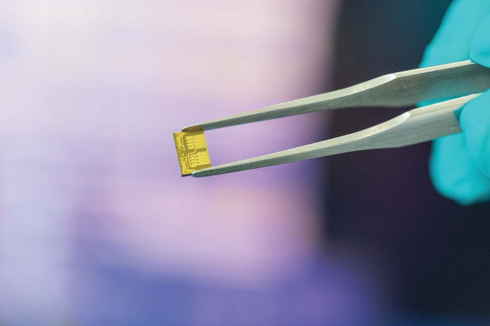
Photonic integrated circuits (PICs) integrate optical functions (generation, modulation, routing, detection, and, increasingly, computation) onto chips. As bandwidth demand grows and power budgets shrink, the industry is steadily pushing photonic interconnects closer to the silicon: from the global network backbone all the way down to the package, to the dies themselves, and between chiplets in a package. That shift is not just a bullet point on a roadmap. It changes, fundamentally, how semiconductors get tested and built. In most PIC workflows today, the bottleneck is no longer the optical design; it’s the packaging. Physik Instrumente (PI) addresses this head-on with precision motion subsystems and alignment firmware that turn what used to be slow, serial active alignment steps into fast, repeatable, factory-grade processes.
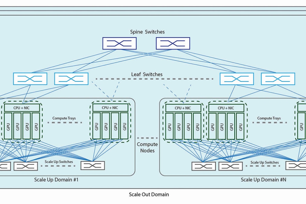
From transoceanic links to chip-to-chip optics: a compressed history Photonics started at the largest scales: transoceanic and transcontinental fiber networks that made long-distance communication viable. From there, the frontier moved steadily inward through regional and metro networks, then fiber-to-the-home, each step shrinking the span while multiplying the endpoints. The next jump brought photonics inside the data center, replacing copper in building-to-building links and rack-to-rack connections.
Now the industry is pushing further still: co-packaged optics (CPO) and related architectures aim to place optical components on the same substrate as switching or compute silicon, cutting electrical trace lengths and the power and signal losses that come with them. The appeal is real: better power-per-bit, higher capacity and lower latency by moving optical conversion right up next to the ASIC. [R5] [R6] [R7]
AI is accelerating this. Training and inference clusters generate massive east–west traffic, while power and cooling have become first-order design constraints rather than afterthoughts. Latency, once a secondary concern, is now a competitive differentiator, especially in disaggregated architectures and edge AI deployments. Meanwhile, the ambitions for optical interconnects keep expanding outward too: low-Earth-orbit networking and ‘data centers in space’ concepts are gaining traction as routes to unique power and cooling environments. Whether those particular visions pan out or not, the broader signal is unmistakable: PIC-enabled interconnects are evolving into a cross-scale platform, from chiplets in a package all the way to global links. The common thread running through all of it is manufacturable, high-yield optical coupling.
PIC interconnects inside the package: chiplets, CPO, and the
war on latency
Inside advanced packages, PICs appear in two main configurations. First, optical engines sit adjacent to compute or switch on silicon (the CPO model). Second, as photonic bridges between chiplets (think memory accelerator links) where electrical channel limits and power density make optical alternatives attractive. Both approaches rely on dense arrays of optical I/O, often tens of channels at once, which immediately sets up the assembly challenge: you need to align arrays of fibers, lenslets, interposers, or waveguide couplers with sub-micron accuracy without sacrificing production throughput. Every review of photonic-chip packaging says the same thing: optical I/O coupling and interconnection are the central scaling challenges. [R8]
From a manufacturing perspective, the uncomfortable truth is that packaging and testing often dominate both time and cost, especially when legacy active alignment is used as a serial, single-channel process. As channel counts climb, the penalty compounds: more elements to align, more degrees of freedom to optimize, and more repetitions across wafer test, module assembly, and final package verification. A small inefficiency in alignment becomes a hard capacity and yield ceiling at volume. That’s why ‘alignment economics’, not just alignment accuracy, has become a strategic lever for anyone running a serious PIC program.
From a technical perspective, our use of the word “accuracy” regarding alignment performance spotlights the additional need for an evolved vocabulary for this field. Ordinarily, accuracy regards the performance of a positioner versus a perfect ruler. This goes to manufacturing quality, encoder principle, and other mechanical subtleties, and can be seriously impacted by design choices like fixturing offsets and environmental variables such as temperature. In the context of alignment, however, accuracy reflects the ability of the system to determine the mutual position and orientation that achieves best coupling according to the figure of merit (usually, but not always, optical power). This goes more to the alignment system’s algorithms than its physical details. In fact, highly accurate alignment can be achieved with open-loop mechanisms lacking any motion metrology at all, as was the case for the earliest active alignment engines in the late 1980s.
The recurring challenges - and how PI addresses them Yield: coupling accuracy, drift control, and device safety
Yield in the PIC assembly is tightly coupled to positioning accuracy. Coupling losses can escalate significantly with even small offsets, particularly for edge coupling and other tight mode-field interfaces where the tolerances leave little room for error. PI’s active alignment approach treats coupling as a closed-loop optimization problem: measure optical power (or another figure of merit) in parallel with multi-DOF motion, converge on the optimum, then hold it. This is spelled out clearly in PI’s own active alignment publications and documentation, which identify silicon photonics testing and packaging as key drivers for both nanoscale accuracy and economic efficiency. [R1]
PI’s Fast Multichannel Photonics Alignment (FMPA) systems
bring precision mechanics together with intelligent, firmware-level alignment
commands running in dedicated digital controllers (the E-713 platform being the
flagship example) to enable fast, simultaneous alignment and tracking of
multichannel couplings across multiple degrees of freedom (DOFs) and multiple
inputs and outputs. [R2] [R9]
There’s also a practical device safety benefit to this architecture. By integrating motion, sensing, and alignment logic inside the controller itself, systems can execute scans efficiently, without the stop-start latency of PC-mediated control loops, while operating within well-defined constraints. When you’re dealing with expensive wafers or fragile fiber arrays, that predictability matters as much as raw speed.
Productivity: throughput, reproducibility, and new
approaches
Throughput matters enormously in PIC manufacturing. Alignment steps repeat constantly, and as channel counts keep rising, any slowness in that step compounds. PI reports that FMPA can cut fiber-array alignment time in silicon photonics packaging by roughly a factor of 100, down to about one second, compared to conventional approaches. [R3]
But this isn’t purely a speed story; it’s a reproducibility story. When alignment is automated and embedded in the motion control stack, the result depends less on operator skill and more on traceable control parameters. That creates a pathway to process capability metrics, recipe management, and scalable QA: exactly the kind of rigor the semiconductor industry already expects in front-end manufacturing.
Worked examples: FMPA, PILightning, and PINovAlign
Example A: Multichannel optimization: Once multichannel PICs became the norm, aligning fibers became an obvious bottleneck; you could see it in cycle times. There are several reasons: foremost is simple geometric dependencies between DOFs, where adjustment of one axis impacts others.
Formerly, a recursive, looping, and serial approach was required to bring everything into consensus alignment. This was time-consuming. PI’s FMPA was designed specifically to address this, enabling parallel optimization across channels and degrees of freedom simultaneously, all implemented at the firmware level in PI’s controllers. [R2] [R10]
Example B: Time to ‘first light’: Getting to that initial coupling point is often the most painful part of active alignment, particularly when tolerances are tight and the search space is large. PI’s PILightning feature extends the FMPA algorithm package specifically to accelerate this initial acquisition phase and improve overall alignment efficiency on compatible controller platforms. [R4]
Example C: Compact, cost-optimized alignment: Not every station needs a full hexapod, and PI recognizes that. The PINovAlign (F-141) is aimed at applications that need fast, accurate multi-axis motion in a compact footprint: a cost-optimized system with fast alignment algorithms baked in, purpose-built for PIC test and assembly environments [R11] [R12]
Trends shaping PIC assembly and why general solutions still
work
PIC device diversity is relentless: grating couplers, edge couplers, integrated lasers, externally coupled sources, photodiodes, phased arrays, interposers, new fiber types, and the list keeps growing. It’s the fundamental reason for the field’s lack of standards. The formats evolve, but the underlying physics stays consistent. Most coupling problems come down to finding either a clear optimum (a peak in received power) or a centroid computable from sensor data. That’s why a well-designed general alignment engine that can scan, evaluate a merit function, and optimize across multiple axes translates across a wide range of PIC products even as device geometries change year to year.
PI reinforces this generality through modular motion and control building blocks: stacked linear stages for XYZ travel, rotary axes for theta adjustments, and parallel-kinematic platforms (hexapods). On the control side, the E-713 motion controller supports synchronous, high-precision operation across up to 16 logical axes with mixed drive types, giving tool builders the flexibility to scale their architectures as products evolve. [R9]
Passive alignment motivation and why active alignment matters more than ever
The multi-decade interest in passive alignment approaches makes sense as a reaction to legacy active alignment’s well-known slowness.
Companies like Teramount are building around wafer-level self-aligning optics and wider assembly tolerances to enable higher-volume packaging with more conventional assembly lines. [R13] [R14]
But passive and active alignment are not actually at odds. Many products still need at least one active alignment step, or at minimum an active verification step, to account for real-world variability and squeeze out maximum coupling efficiency. And honestly, much of the push toward passive alignment is a pushback against outdated active alignment workflows specifically.
Modern active alignment, with parallel optimization, fast
scans, and embedded control logic, changes the cost equation considerably. PI
makes this explicit: the evolution from manual single-fiber methods to fully
automated array alignment is a continuum, and modern tooling can combine
passive placement with high-speed active optimization wherever that combination
makes sense. [R15]
Adjacent semiconductor subprocesses where PI’s capabilities
translate
PIC packaging and test lines function as interconnected elements of broader advanced-packaging flows, not as discrete, independent processes. Several neighboring subprocesses draw on exactly the same core competencies PI brings high-precision pick-and-place, metrology and inspection positioning, lithography-related alignment. In most of these contexts, tool architects want coarse-fine implementations: long travel approach moves and format changes, then high-resolution nanopositioning for final alignment and drift compensation. PI’s photonics alignment systems are built around hybrid mechanisms specifically designed to deliver long travel without trading away stability, resolution, or alignment speed. [R2]
Tooling architecture: flexibility, modularity, and EtherCAT-based scalability One underappreciated constraint in PIC manufacturing equipment is architectural longevity. Tool builders and in-house integrator teams need platforms that can scale in axis count, support mixed actuator types, and stay serviceable across multiple product generations, not just for the device they’re shipping today. Industrial fieldbuses like EtherCAT are a proven way to achieve deterministic multi-axis control while keeping the architecture modular and expandable.
PI highlights EtherCAT-capable controllers in photonics assembly contexts and positions its software stack to support fast application development across common operating systems and programming languages. [R16]
Looking forward: parallelization, embeddability, and
partnership
Two requirements will be defined in the next phase. The first is parallelization: running more alignment processes simultaneously, whether in wafer-level testers or high-channel-count probe and coupling stations. The second is embeddability: compact form factors that fit inside dense tools and automation cells without giving up dynamic performance. PI’s product and system demonstrators point in exactly this direction, combining proven fiber alignment systems with multi-axis gantry automation to push toward more fully automated fiber array assembly workflows. [R17]
In the end, PI’s value to PIC manufacturing is not any single product; it’s an enabling platform: precision motion, firmware-level alignment intelligence, and scalable tooling architecture working together.
As PIC applications stretch from package-scale integration
toward network and even ‘planet-scale’ visions, the manufacturing challenge
converges on one thing: fast, repeatable, high-yield optical coupling at
ever-higher channel counts. The companies that industrialize alignment, that
make it fast, predictable, and scalable, will define what PIC manufacturing
looks like at volume. PI is building the subsystems and control engines to make
that happen.