Tantala enables 3D PICs

Researchers demonstrate a multilayer photonic platform combining tantala and lithium niobate to generate tunable laser light across visible and infrared wavelengths
Researchers at the National Institute of Standards and Technology have developed a photonic integrated circuit platform that uses tantala to enable tunable laser generation across a wide spectral range.
The work, led by Grant Brodnik, demonstrates how tantalum pentoxide can be integrated with thin film lithium niobate to create a three-dimensional photonic architecture capable of advanced optical functions.
The approach addresses a long-standing challenge in photonics, where combining multiple materials is often limited by thermal and mechanical incompatibilities.
Many photonic applications require stable, narrow-band light sources at specific wavelengths, particularly in the visible range.
However, these systems are typically bulky and confined to laboratory environments due to the difficulty of integrating high-performance light sources on chip-scale platforms.
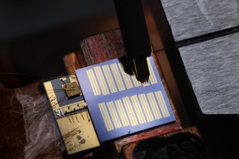
In this work, tantala is deposited at relatively low temperatures and exhibits low internal stress, making it compatible with existing photonic structures.
This allows it to be layered directly onto pre-patterned lithium niobate devices without damaging the underlying circuitry.
The result is a monolithically integrated platform in which multiple photonic layers can interact.
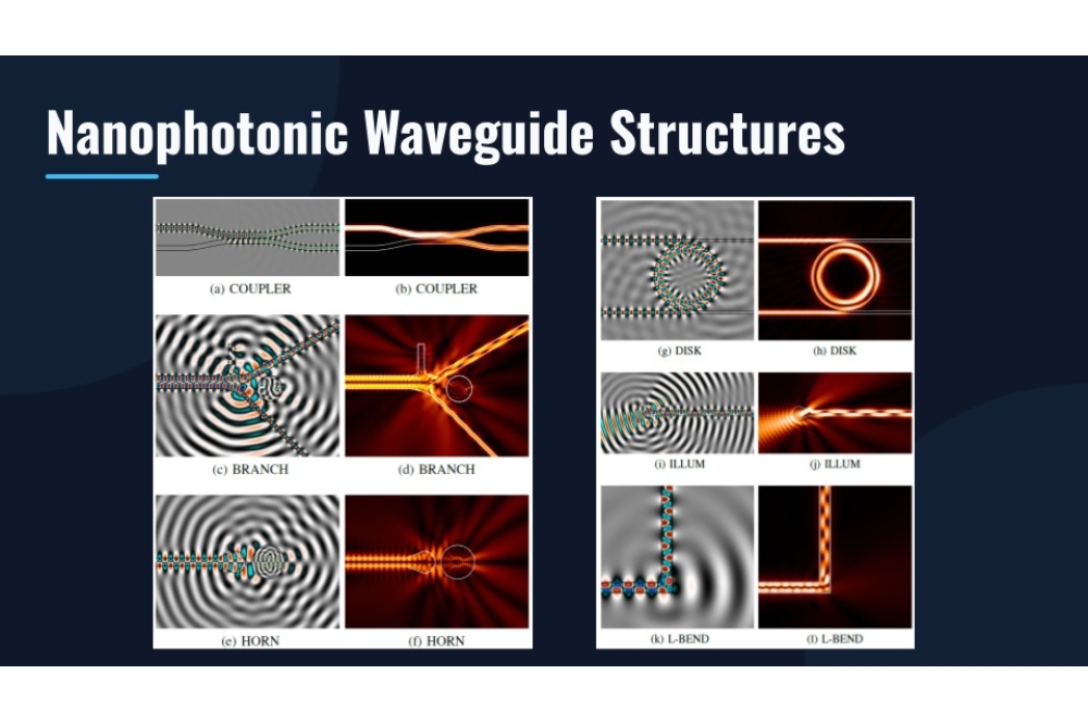
The researchers used this structure to demonstrate a range of functions, including wavelength conversion from infrared to visible light, frequency comb generation, and supercontinuum sources.
In several cases, the tantala layer was used to generate optical pulses that were then processed within the lithium niobate layer, highlighting the complementary roles of the two materials.
The ability to stack photonic materials in this way points toward more flexible and scalable integration strategies.
Rather than relying on a single material platform, designers can combine layers with different optical properties to achieve functionalities that are not possible in isolation.
Such an approach could support the development of compact, low-cost photonic systems for applications in communications, sensing, and precision measurement.
It also reflects a broader trend toward heterogeneous and three-dimensional integration in photonic integrated circuits, where performance gains are increasingly driven by how effectively different materials can be combined.