Siemens and Samsung expand PIC collaboration

The companies are strengthening joint design enablement efforts across photonic IC verification, advanced packaging and 2nm semiconductor technologies.
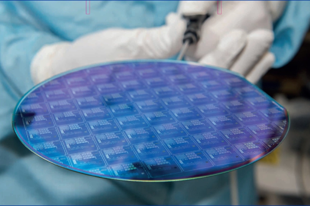
Siemens and Samsung Foundry have expanded their collaboration to support advanced semiconductor design and manufacturing workflows, with new joint efforts spanning photonic integrated circuit (PIC) verification, advanced packaging and leading-edge process technologies.
Announced at the Samsung SAFE Forum 2026, the collaboration includes qualification of Siemens’ electronic design automation (EDA) solutions for Samsung Foundry’s next-generation 2nm processes, alongside support for complex 2.5D and 3D IC designs.
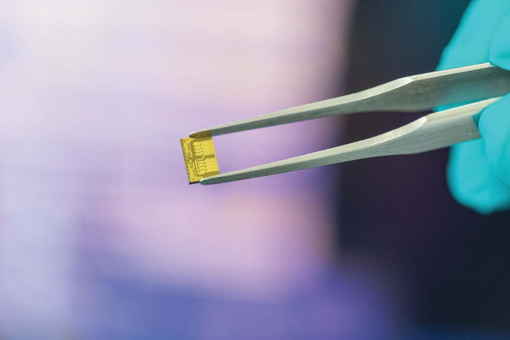
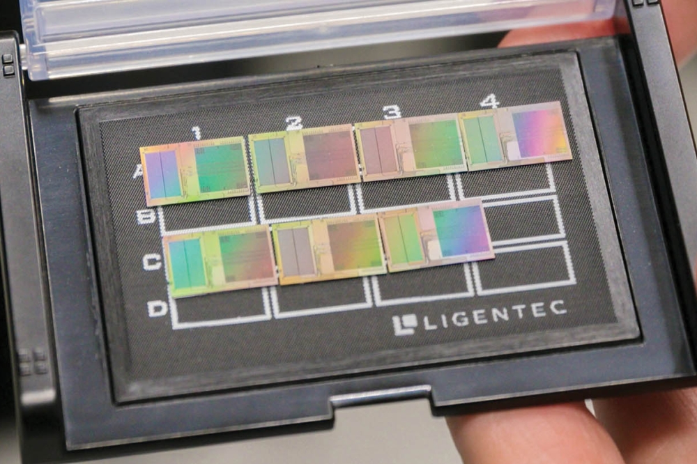
A key focus area is photonic integrated circuit verification, where the companies are working to address increasing photonic design complexity using Siemens Calibre software.
The joint solution supports equation-based design rule checking, curvilinear layout-versus-schematic verification and advanced pattern matching to improve manufacturable PIC design flows within Samsung Foundry processes.
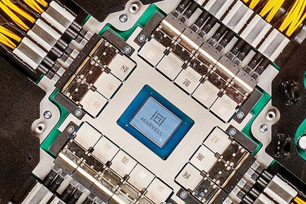
The collaboration also extends to advanced packaging, where Samsung Foundry has adopted Siemens solutions for its 2.3D Cube-E package platform.
The technologies support floorplanning, multi-million pin layout automation and physical verification for complex 2.5D and 3D IC implementations.
Additional work includes design-for-test methodologies, power integrity optimization and analog, RF and digital implementation flows for advanced semiconductor nodes.
The companies said the continued collaboration is intended to help customers address growing design complexity while accelerating development across advanced semiconductor and heterogeneous integration technologies.