Keysight adds GlobalFoundaries PDK

New design flow enables engineers to simulate photonic integrated circuits and validate optical link performance within a single environment.
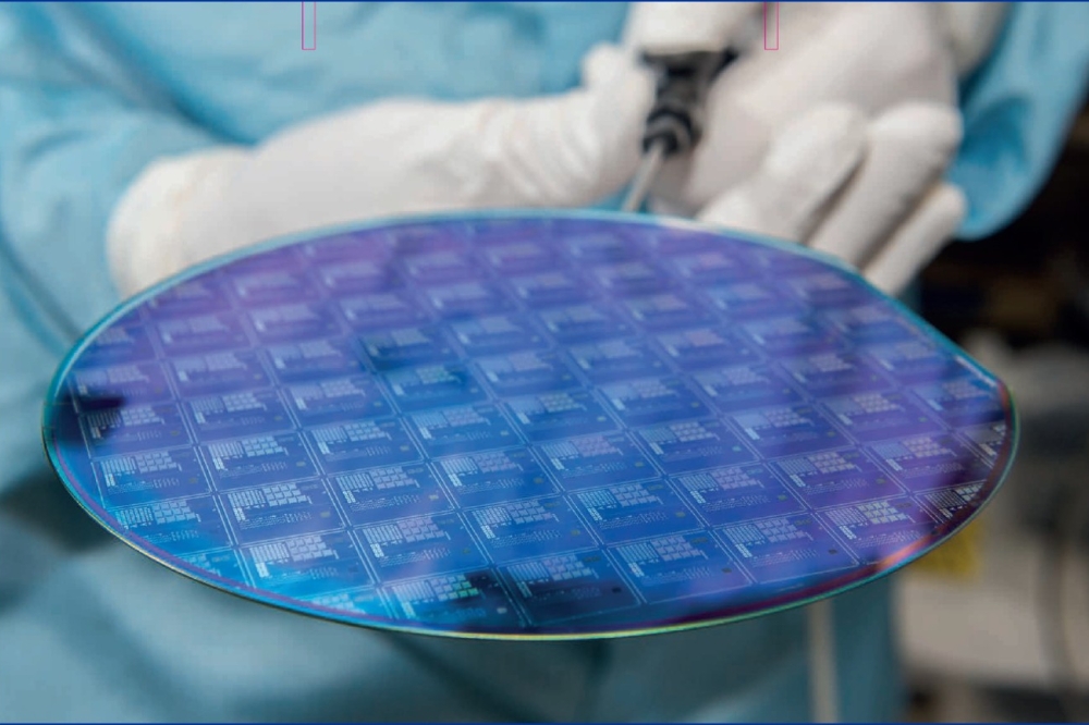
Keysight Technologies has announced support for GlobalFoundries’ silicon photonics process technology in its Advanced Design System (ADS) Photonic Designer, expanding the company’s ecosystem for photonic integrated circuit (PIC) development.
The new process design kit (PDK) enables engineers to design PICs on GlobalFoundries’ silicon photonics platform and validate electro-optical-electrical (EOE) system performance without moving between separate design and simulation tools.
As silicon photonics adoption accelerates across AI infrastructure, optical communications and data centre applications, designers face increasing pressure to verify device performance at both the circuit and system levels before fabrication.
Keysight said its integrated workflow allows engineers to evaluate optical link behaviour, including signal integrity and transmission performance, earlier in the development cycle.
The PDK is built on physics-based models aligned with GlobalFoundries’ silicon photonics manufacturing process, helping designers correlate simulations with fabricated devices while reducing development risk and design iterations.
The solution is aimed at developers of optical transceivers, high-speed optical interconnects and co-packaged optics, where photonic and electronic performance must be optimised together to meet growing bandwidth and power-efficiency requirements.
The GlobalFoundries PDK for ADS Photonic Designer is available immediately.