Building the fab of the future for high volume PIC manufacturing
Photonic integrated circuits are moving from technical
promise to industrial expectation. Customers are no longer asking whether PICs
can work; they expect reliable delivery, traceable quality, and repeatable
performance at scale. For the photonics industry, this marks a decisive shift:
from research excellence to disciplined manufacturing.
For years, the photonic integrated circuit (PIC) industry has been driven by research, prototyping, and technical demonstration. Across Europe, companies, universities, and research institutes have proven that PICs enable powerful solutions in telecom, sensing, LiDAR, medical applications, quantum technologies, and datacentre connectivity. This research phase has created the foundation on which the industry stands today.
However, the demand has changed. It is no longer limited to whether a device can be designed and demonstrated. It is now also about whether PICs can be produced reliably, at acceptable cost and in high volume.
This marks the shift toward industrial maturity. Customers no longer accept demonstrations alone. They expect predictable delivery, controlled processes, full traceability, repeatable quality, and the ability to scale rapidly without losing control of yield or performance. For Tier 1 customers, these are not preferences, they simply demand it.
SMART Photonics is one of the companies navigating this transition. As an independent pure-play InP foundry, it sits at the centre of the lab-to-fab challenge: enabling advanced photonic designs while building the manufacturing maturity required for scalable production. Itility supports this challenge by implementing proven semiconductor principles into a digital and operational backbone.
Market forces driving urgency
The urgency to scale is driven by strong market forces. AI workloads are increasing rapidly, while hyperscale datacentres require faster, denser and more energy-efficient data transfer. As copper-based systems approach their limits, PICs offer a compelling alternative toward higher-bandwidth, lower-power interconnects.

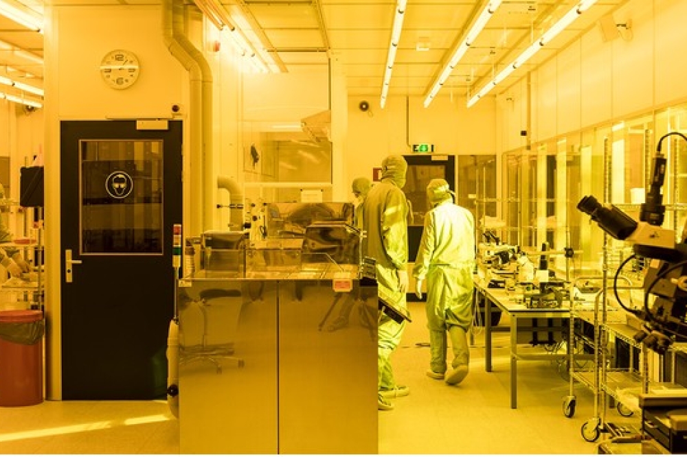
Figure 1: A cleanroom operator working alongside advanced manufacturing equipment in a highly controlled production environment.
Industry expectations point to significant growth, with the PIC market projected to exceed 50 billion USD in the coming decade. Capturing this opportunity requires more than technology alone: it requires a manufacturing model that can deliver PICs with the reliability, repeatability, and discipline seen in high-volume semiconductor environments.
From research mindset to industrial reality
Scaling PIC manufacturing requires a shift in mindset. Many photonics organisations originate from research environments, where flexibility, speed and experimentation are essential. While this heritage is a strength, it becomes a constraint when moving to volume production. For example, in early-stage R&D manual workflows are common, data can be fragmented across tools and teams, tools operate in isolation, and processes depend on individual expertise. Critical knowledge often resides on laptops or in the minds of experienced researchers. This works for rapid experimentation but does not provide the right backbone required for high-volume manufacturing.
Transitioning to industrial manufacturing is therefore not a simple step. It requires time, investment, change management and a structured approach to standardisation, data, and process control. With demand increasing and customer expectations rising, such transformation must start early to ensure timely readiness to scale.
The focus shifts from identifying challenges to building the capabilities required to overcome them. At the core is a strong data foundation: data must be complete, consistent, and accessible across the organisation, enabling a single, trusted view of operations and faster decision-making. Standardised workflows and well-defined processes are equally critical. Alignment on internal practices and use of industry standards ensures repeatability, comparability, and scalability, forming the basis for consistent manufacturing performance.

Figure 2: Projected growth of the Photonic Integrated Circuit market, driven by rising demand for faster data transmission.
Design, manufacturing and testing systems should function as a connected toolchain that provides end-to-end visibility and enables insight into process and equipment behaviour. A further key step is the transition from individual-driven expertise to structured, organisation-wide knowledge. Design methodologies, process know-how and best practices must be captured and shared, reducing dependency on individuals. Together, these elements mark the shift from flexible R&D to disciplined manufacturing.
SMART Photonics is an independent pure-play Indium Phosphide (InP) foundry based in Eindhoven, the Netherlands. Founded in 2012 as a spin-off from TU Eindhoven and Philips, the company was created to make advanced Indium Phosphide photonic integration technology available through a foundry model. Smart’s InP platform is especially relevant because it enables active optical functions, such as lasers and amplifiers, to be integrated with other photonic components on the same chip. Over the years, SMART has grown from an R&D-driven photonics company into an important player in Europe’s integrated photonics ecosystem, serving applications in data and telecom, sensing, LiDAR, and medical technologies. Its current journey reflects the wider challenge facing the industry: moving from innovation and early production toward mature, reliable, and scalable high-volume PIC manufacturing.

Figure 3: Wafer-level image of an InP Photonic Integrated Circuit, combining active optical components, waveguide routing, and metal interconnects.
For a foundry as SMART Photonics, scaling is not only about producing more wafers. It means strengthening the full operating model across design enablement, manufacturing processes, equipment data, product qualification, testing, quality control, and customer delivery. SMART’s transformation is therefore a practical example of the shift needed in the photonics industry.
From ambition to execution: Building maturity in practice
SMART Photonics has the ambition to operate as a Tier 1 photonics foundry. In practice, this means meeting customer expectations on predictable delivery, quality, traceability, and scalability. The semiconductor industry offers a valuable reference model. Decades of high-volume chip manufacturing have created mature practices in design, automation, process control, equipment integration, quality systems, traceability, and yield learning. However, these practices cannot simply be copied into photonics. PIC manufacturing has its own materials, process sensitivities, and test requirements.

The challenge therefore lies in translating semiconductor best practices into photonics context. This translation must be practical and incremental. It starts with controlled workflows, reliable data capture, and standardised processes, and then evolves toward integrated systems, automated execution and closed feedback loops across design, manufacturing, and test.
This is where Itility supports SMART Photonics. Itility brings 20+ years of experience in high-tech and semiconductor manufacturing environments, combining software engineering, data platforms, automation, cloud infrastructure, and secure engineering workflows. Together, SMART Photonics and Itility translate these foundations into an executable maturity roadmap for high-volume PIC manufacturing. Rather than a one-time transformation, this roadmap describes a step-by-step evolution moving fully away from manual, person-dependent ways of working toward standardised processes, automated equipment, and real-time data availability.
Itility is a digital engineering consulting company headquartered in Eindhoven the Netherlands, with a strong presence in high-tech manufacturing and the semiconductor industry. The company supports customers translate technology into practical business and operational value by building customer-specific solutions using software, automation, data, cloud, and AI. Itility is renowned for working closely at customers to truly understand their processes and develop solutions that improve how teams operate, make decisions, and achieve higher maturity levels following industry best practices.

As maturity increases, data becomes structured and integrated across the organisation. This results in reusable blueprints, consistent execution and advanced capabilities as automated decision-making and AI-assisted engineering. The goal is not automation for its own sake, but controlled scaling: increasing output while improving predictability, quality, and speed of learning. In a mature PIC foundry, design, manufacturing, and testing are tightly interconnected. Design defines what is built, manufacturing determines how it is produced, and testing provides the feedback needed to continuously improve both. In the following sections, we will explore how each of these three core processes enable scalable, data-driven photonics manufacturing.
Core process 1: Design as a foundry discipline (EDA as backbone)
In high-volume PIC manufacturing, design is not an isolated creative activity. It is a foundry discipline that extends from PDK governance and customer design verification, to controlled tape-out and feedback from manufacturing and test.

Figure 4: From ambition to execution: combining SMART Photonics’ PIC manufacturing expertise with Itility’s digital engineering capabilities to build a maturity roadmap for high-volume PIC manufacturing.
A PIC foundry does more than manufacture customer layouts. It develops, maintains, and qualifies its own building blocks that customers use to create functional circuits. These building blocks are brought together in a Process Design Kit (PDK), which includes libraries, design rules, technology data, layout constraints, and simulation models. The PDK enables customers to develop manufacturable designs that align with the foundry process. Its maturity directly affects first-time-right design, manufacturability, yield learning, and customer confidence.
For this reason, the PDK must be treated as a controlled asset. Changes to building blocks, design rules or models need to be governed, versioned and traceable. Customers and internal engineering teams must work with consistent libraries and qualified workflows. Without this discipline, design freedom can easily translate into process risk, especially as volumes increase and more customers depend on the same foundry platform.
Tape-out is the critical handover point between design intent and manufacturing execution. In a mature foundry environment, tape-out cannot be treated as an administrative step toward mask creation but is a controlled release process.
To ensure quality and scalability, this entire process must be supported by a semicon industry best practice: an Electronic Design Automation (EDA) environment, which acts as the backbone of all design activities. First, it provides a secure collaboration environment for working with sensitive data, including customer IP and the foundry’s own building blocks. Second, it creates a consistent and managed workspace for engineers, where tools, libraries and workflows are made available in a controlled way. This allows engineers to focus on design quality rather than design tool configuration or version management. Third, it acts as a platform for structured verification, simulation, and automation.
The real value emerges when this design environment is connected to manufacturing and test data. Insights from the fab and test floor can be fed back into design rules, building blocks and simulation models. Over time, this creates the foundation for high-yield manufacturing by using advanced capabilities in design optimisation, automated verification, and AI-supported design workflows. This is what data-driven steering means in practice: not adding AI as a standalone feature, but first building the secure, connected, and automated design foundation that allows AI to create real value.
Core process 2: Manufacturing powered by data
Reliable, high-volume PIC production requires manufacturing to be supported by trusted operational data. In a mature fab environment, reliance on manual tool settings, individual expertise or fragmented reporting is no longer appropriate. Engineers and operators need access to the right information at the right time to understand process behaviour, equipment performance and execute actions in a standardized order on the shop floor.

Figure 5: A close-up view of an integrated circuit, where compact optical components are brought together on a single chip.

Figure 6: A cleanroom environment with operators and equipment used for high-precision manufacturing and process control at Smart Photonics
In practice, this means actively supporting operators through intuitive interfaces, uniform instructions, and automated guidance, while ensuring that equipment recipes and configurations are automatically selected and consistently enforced for each wafer and process step. This reduces variability and human error, enabling repeatable execution across the fab. To reach this level of control, semiconductor best practices play a key role, requiring clear visibility into equipment behaviour, process performance and production flow, combined with the ability to translate this insight into effective actions, including taking the right corrective measures when deviations occur. Here an MES layer is essential to manage and optimise execution on the shop floor, delivering end-to-end traceability and data-driven process control. By adhering to the ISA‑95 framework, it establishes a clear interface between business systems and manufacturing operations, enabling standardisation and future scaling.
With this foundation in place, the focus shifts from data collection to insight and control. Statistical Process Control (SPC) enables early detection of process variation and prevents drift before it impacts product quality. Overall Equipment Effectiveness (OEE) complements this by providing insight into availability, performance, and utilisation, allowing teams to track productivity and steer improvements through clearly defined KPIs.
To make this effective, manufacturing must be built on an end-to-end data integration strategy. The objective is not to build isolated dashboards or point solutions, but to create a structured data foundation that connects equipment, process, wafer, product, and quality information. This enables engineers to analyse process behaviour, identify bottlenecks and act on deviations with greater speed and confidence.
A practical way to implement this is through reusable blueprints. Instead of building isolated solutions for each tool or process, standardised templates can be applied across similar equipment and setups. These blueprints define interfaces, integrations, and data flows, ensuring consistent execution and enabling structured monitoring across the fab.
As manufacturing maturity increases, the fab evolves from retrospective reporting to proactive control. Insights are no longer used only after the fact; they are fed back into operations to support faster intervention, more stable processes, and more predictable output. This is the route toward scalable PIC manufacturing: not more data for its own sake, but data that directly improves control, quality, and throughput.
Core process 3: Testing as the scaling engine
In high-volume PIC manufacturing, testing cannot be treated as the final checkpoint at the end of the process. It is a scaling engine. Testing is where design intent, process behaviour and product performance come together, and where the foundry learns whether its platform can deliver repeatable results at volume. In this way, it actively steers the full process flow. It supports yield improvement and enhances equipment productivity and enables a shift from experience-based decisions to consistent, data-driven control.
The first step toward higher maturity in testing is automation of test execution and data processing. Manual validation, inconsistent test setups, and fragmented result files create delays and uncertainty. Automated test workflows, calibrated measurement routines, and built-in data verification allow engineers to trust the data and act immediately. This reduces the need for retesting, shortens learning cycles, and improves the efficiency of engineering and production teams.
As test data quality and trust improve, testing becomes a feedback mechanism for both manufacturing and design. Measurement results can reveal process drift, layout sensitivities, building block behaviour, and product-specific yield patterns. These insights can then be fed back into process control, PDK updates, design rules, and simulation models. This changes the role of testing fundamentally. Instead of confirming quality after production, testing actively steers yield improvement and platform maturity.
Over time, better test automation and stronger data correlation reduce the overall test burden. Test times are shortened, retesting becomes less frequent, and discussions on data validity also diminish. This is not only an efficiency gain, but essential for meeting customer expectations in speed, reliability, and traceability.
In a mature PIC foundry, testing closes the loop across design, manufacturing, and product qualification, enabling faster optimisation cycles and creating the confidence needed for scalable high-volume production.
The hard truth: you cannot scale photonics in isolation
Even if a foundry executes perfectly, scaling PIC manufacturing will inevitably expose constraints elsewhere in the value chain. High-volume photonics is not only a fab challenge. It is a system-level industrialization challenge.
Upstream, material availability and supplier maturity can become limiting factors, particularly for specialised substrates (such as InP wafers). As volumes continue to grow, bottlenecks typically shift downstream into testing, packaging, and assembly. These are often device-by-device processes, making them similarly difficult to automate and scale.
The challenge becomes even more critical with heterogeneous integration between photonics and electronics, such as in co-packaged optics. In these cases, performance and reliability must be verified within the fab flow before permanent integration since failures after integration are significantly more expensive and difficult to resolve.
Scaling photonics therefore requires the full ecosystem to mature together. Foundries, design houses, EDA providers, equipment suppliers, material suppliers, packaging partners, OSAT providers, system integrators and investors all play a role. If one part of the chain matures while others lag, bottlenecks will not disappear; they will simply move.
One potential consequence is that the industry may move towards more vertically integrated models, in contrast to the mature horizontal semiconductor ecosystem optimised for massive volumes, speed and innovation.
For Europe, this is a critical opportunity and a critical test. The region has strong photonics research, leading equipment expertise, specialised foundries, and an active ecosystem around integrated photonics. But industrial leadership will depend on more than technical excellence. It will require alignment on standards, interfaces, qualification methods, data exchange, and investment in scalable manufacturing infrastructure.
The concept of the “fab of the future” is therefore not a single breakthrough, but a disciplined and structured journey. Those who start this journey early and do so together with the right partners and support across the value chain, will be best positioned to capture the full potential of photonic integrated circuits at scale.
Credit: Itility / SMART Photonics