Synopsys launches multiphysics fusion

New design solutions combine multiphysics analysis across digital, analogue, photonic and multi-die workflows to address growing semiconductor design complexity.
Synopsys has introduced its Multiphysics Fusion portfolio, a new suite of design solutions aimed at helping semiconductor engineers manage the increasing complexity of advanced chip development.
The platform integrates electronic design automation (EDA) technologies with Ansys analysis tools, enabling designers to account for factors such as power integrity, thermal effects, electromagnetic interference and mechanical stress within a unified workflow.
The launch comes as advanced process nodes, chiplet architectures and co-packaged optics drive the need for more comprehensive design methodologies.
Traditional approaches often analyse these effects separately, increasing the risk of overdesign and late-stage validation challenges.
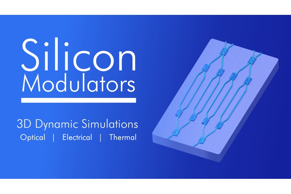
The initial release includes solutions for timing sign-off, design closure, multi-die integration, and analogue and photonic design.
Synopsys said the tools provide system-level visibility across electrical, thermal and electromagnetic behaviour, helping engineers identify issues earlier in the development cycle.
The portfolio also supports the co-design of photonic integrated circuits alongside electronic components, reflecting growing demand for integrated electronic-photonic systems in AI, high-performance computing and next-generation communications.
According to Synopsys, the solutions leverage artificial intelligence and GPU acceleration to improve simulation performance and reduce development time as semiconductor designs become increasingly heterogeneous and complex.