SMART Photonics advances InP PIC scaling

SMART Photonics highlights the advantages of indium phosphide (InP) photonic integrated circuits and outlines its roadmap toward large-scale manufacturing, supporting growing demand from AI, datacom, and sensing applications.
SMART Photonics has highlighted the growing importance of indium phosphide (InP) photonic integrated circuits (PICs) in meeting the performance and efficiency demands of emerging applications such as artificial intelligence, data communications, and sensing.
In a discussion with PhotonDelta, the company emphasized that InP remains the only photonic platform capable of integrating light generation, modulation, detection, and transmission on a single chip, enabling compact and energy-efficient optical systems.
The company also underscored the role of its Process Design Kits (PDKs), which include more than 50 validated photonic building blocks developed over a decade of manufacturing experience.
These standardized components help designers accelerate PIC development while reducing complexity and risk.
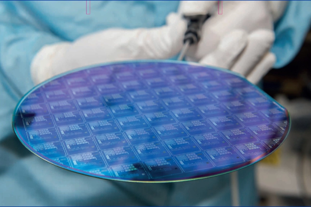
Looking beyond prototyping, SMART Photonics outlined its efforts to scale manufacturing capacity through larger wafer sizes and improved production processes.
In collaboration with TNO and as part of the PIXEurope initiative, the company is developing a 6-inch pilot production line at the High Tech Campus Eindhoven.
Expected to be completed around 2027–2028, the facility is projected to produce approximately 10,000 wafers annually, supporting the manufacture of millions of photonic chips.
As an independent foundry, SMART Photonics enables customers to retain ownership of their intellectual property while accessing mature manufacturing infrastructure and expertise.
The company believes that advances in foundry capabilities, design ecosystems, and industry collaboration will continue to accelerate the adoption of integrated photonics across a broad range of markets.