Keysight expands photonics portfolio

The acquisition expands Keysight's photonic design automation capabilities, adding system-level simulation to support the growing demands of silicon photonics, co-packaged optics and AI infrastructure.
Keysight Technologies has completed its acquisition of VPIphotonics, expanding its photonic design automation portfolio with system-level simulation capabilities and strengthening its position in the rapidly growing silicon photonics market.
The acquisition, completed on June 9, extends Keysight's photonic design workflow from device-level modelling through to full optical system simulation, enabling engineers to evaluate complete optical links within a unified design environment.
The move comes as demand for silicon photonics and co-packaged optics continues to accelerate across AI infrastructure and data centre applications.
As optical systems become increasingly complex, developers face growing pressure to reduce design cycles and improve integration between electrical and photonic domains.
Keysight's photonic design automation portfolio already includes RSoft for device-level simulation and Photonic Designer for photonic integrated circuit (PIC) design and verification.
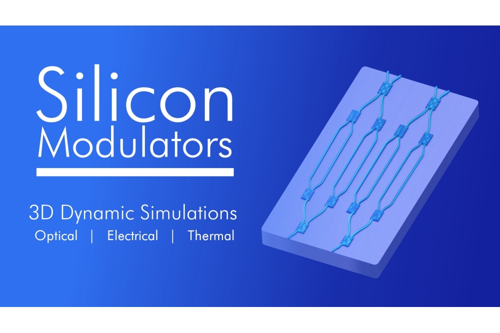
The addition of VPIphotonics Design Suite introduces system-level modelling capabilities, allowing engineers to analyse the performance of complete optical communication systems alongside individual photonic components.
One key capability highlighted by the company is VPI Optical Link in Keysight ADS, which enables simulation of an entire transceiver chain from electrical signals to optical transmission and back to electrical detection within a single workflow.
This approach allows designers to predict system-level metrics such as bit error rate while reducing the need to transfer designs between separate software environments.
The integrated workflow also connects simulation results with Keysight's high-speed digital design tools and test instrumentation, helping engineering teams identify performance issues earlier in the development process and reduce prototype iterations.
"Photonics design complexity continues to increase for our customers, especially for those working at speeds greater than 1 THz," said Nilesh Kamdar, General Manager of Keysight EDA. "Having a complete suite of tools that address these challenges from device to system is crucial."
For the photonics industry, the acquisition reflects a broader trend towards electronic-photonic co-design as next-generation AI clusters, optical interconnects and co-packaged optics demand increasingly sophisticated design methodologies.
By combining device, circuit and system-level simulation within a single ecosystem, Keysight aims to provide a more comprehensive workflow for engineers developing advanced photonic integrated circuits and optical communication systems.
As AI infrastructure scales and bandwidth requirements continue to rise, integrated photonic design environments are becoming an increasingly important part of the silicon photonics development ecosystem.