Chiplets redefine AI hardware

An industry review highlights how chiplet architectures, advanced packaging and co-packaged optics are reshaping semiconductor design to meet the growing performance demands of AI and high-performance computing.
Chiplet-based architectures are rapidly transforming semiconductor design, with advanced packaging technologies enabling higher performance, improved yields and greater flexibility for AI, high-performance computing and next-generation networking applications.
In an industry analysis published by EEWorld Online, Advanced Packaging Technologist Joshua Rubin outlines how chiplets have evolved from traditional multi-chip modules into highly integrated systems supported by technologies such as 2.5D and 3D packaging, hybrid bonding, silicon interposers and high-bandwidth die-to-die interconnects.
The article notes that advanced packaging has become a key enabler for chiplet adoption, allowing heterogeneous integration of logic, memory, analog, RF and photonic devices while improving power efficiency and reducing development costs.
Open interconnect standards, including Universal Chiplet Interconnect Express (UCIe), are also accelerating the development of interoperable chiplet ecosystems.
The report identifies AI accelerators, high-performance CPUs and high-bandwidth memory (HBM) as major drivers of chiplet adoption, with leading semiconductor companies increasingly relying on advanced packaging to overcome the limits of traditional monolithic chip scaling.
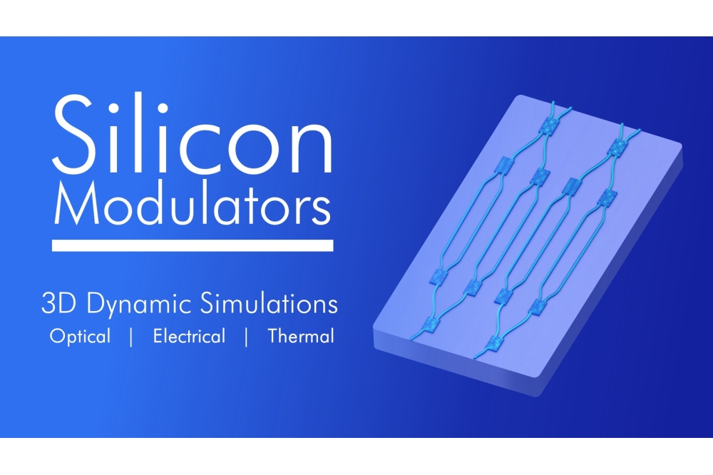
For the photonics industry, the analysis also highlights the growing role of co-packaged optics (CPO), where photonic integrated circuits are integrated alongside electronic chips within advanced packages to deliver higher bandwidth and lower power consumption for AI infrastructure.
The emergence of optical chiplets and UCIe-enabled optical interfaces is expected to further accelerate adoption of CPO in future data centre systems.
Looking ahead, the report suggests that continued advances in advanced packaging, chiplet standardisation, hybrid bonding and wafer-scale integration will reshape package, board and system design as semiconductor manufacturers scale increasingly complex AI hardware.