Transfer printing paves the way for advanced photonic integrated circuits

A new review in Light: Science & Applications highlights transfer printing (TP) as a powerful solution for integrating active optical devices into photonic integrated circuits (PICs).
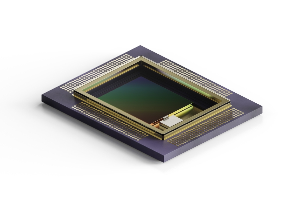
Led by Academician Lijun Wang at the Changchun Institute of Optics, Fine Mechanics, and Physics, the paper explores how TP enables the printing of scale III-V devices, such as lasers, optical amplifiers, and photodetectors, micro and nanoscale onto silicon and silicon nitride platforms.
By precisely controlling adhesion forces with viscoelastic stamps, TP enables the pre-testing of devices, achieves high alignment accuracy, minimises thermal processing, and facilitates cost-effective integration.
Silicon photonics is already widely used in telecommunications, sensing, and quantum technologies, but its inability to generate or amplify light natively has limited full-scale PIC functionality.
Traditional methods like epitaxial growth, wafer bonding, and flip-chip integration involve trade-offs in performance, cost, or scalability. TP combines the strengths of these approaches while reducing their drawbacks, making it suitable for high-throughput heterogeneous integration.
The review provides a comprehensive overview of TP techniques and their applications, showing how they have successfully integrated high-performance components and expanded the capabilities of PICs. This advancement could accelerate the development of dense, multifunctional, and commercially viable photonic chips.