Wide-Area photonic circuits improve terahertz detection

Wide-area photonic integrated circuits enable high-sensitivity terahertz detection and precise beam profiling, paving the way for scalable imaging, sensing, and next-generation wireless applications.
Researchers have developed wide-area photonic integrated circuits that significantly improve terahertz detection and beam profiling, addressing long-standing challenges in the terahertz frequency range.
Terahertz waves, which lie between microwave and infrared frequencies, have strong potential in communications, imaging, and spectroscopy but remain difficult to detect and control using conventional technologies.
The new photonic circuits overcome these limits by enabling large-area integration with high sensitivity and precision.
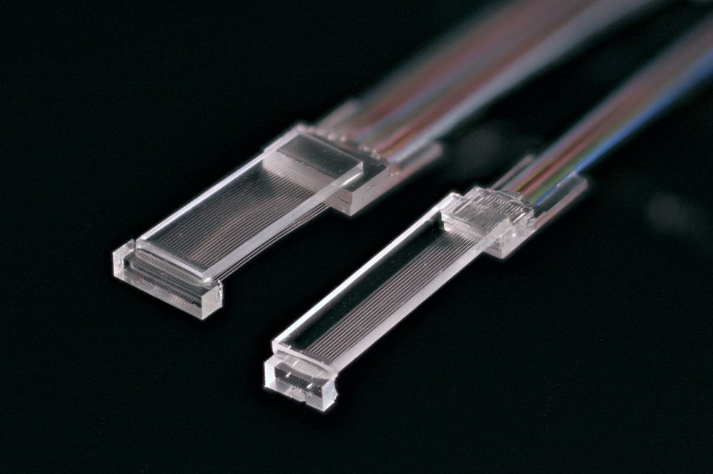
Unlike earlier microscale devices, the circuits cover larger areas while maintaining performance. This allows accurate mapping of terahertz beam intensity and spatial profiles, which is essential for imaging and diagnostic applications.
Advanced coupling designs improve interaction between terahertz waves and on-chip photonic elements, reducing losses and improving signal quality.
Fabricated using high-precision processes and low-loss materials, the circuits operate across broad terahertz bandwidths and remain stable under varying environmental conditions. Experimental results show high signal-to-noise ratios and reliable beam reconstruction.
The technology is compatible with standard photonic and CMOS manufacturing, supporting scalable production. Applications include terahertz imaging, sensing, and next-generation wireless communications, bringing practical terahertz systems closer to real-world deployment.