Breakthrough transfer printing techniques enable next-generation 3D photonic integration

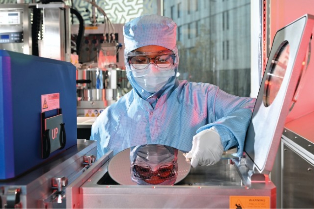
Researchers are pushing the boundaries of photonic device assembly with new transfer printing (TP) techniques designed to place delicate components onto flexible and curved surfaces with far greater accuracy and safety. These methods address long-standing challenges in handling fragile photonic structures and open new opportunities for advanced PIC manufacturing.
A key development is the liquid-droplet stamp, which uses a controlled fluid bridge to gently lift thin semiconductor films such as micro-LEDs without introducing mechanical stress. This allows precise placement on flexible substrates and supports the rise of wearable and bendable optoelectronic devices.
Further expanding 3D capability, inflatable elastomeric balloon stamps conform to curved surfaces through pneumatic pressure, enabling reliable transfer of photodetectors and silicon solar cells onto non-planar geometries. Similarly, a wrap-like petal stamp can envelop spherical objects to print antennas, solar cells and LED arrays, offering a powerful route to curved electronics.
Another promising approach uses shape-memory polymer blocks, which reshape when heated to pick up and place devices with programmable precision.
Collectively, these breakthroughs mark a shift from traditional flat-surface processes toward highly versatile 3D assembly. For the photonics industry, they unlock new possibilities for curved PICs, flexible optoelectronics and next-generation wearable systems, moving advanced photonic integration closer to commercial reality.