Technical Insight
Putting the UK at the forefront of silicon photonics
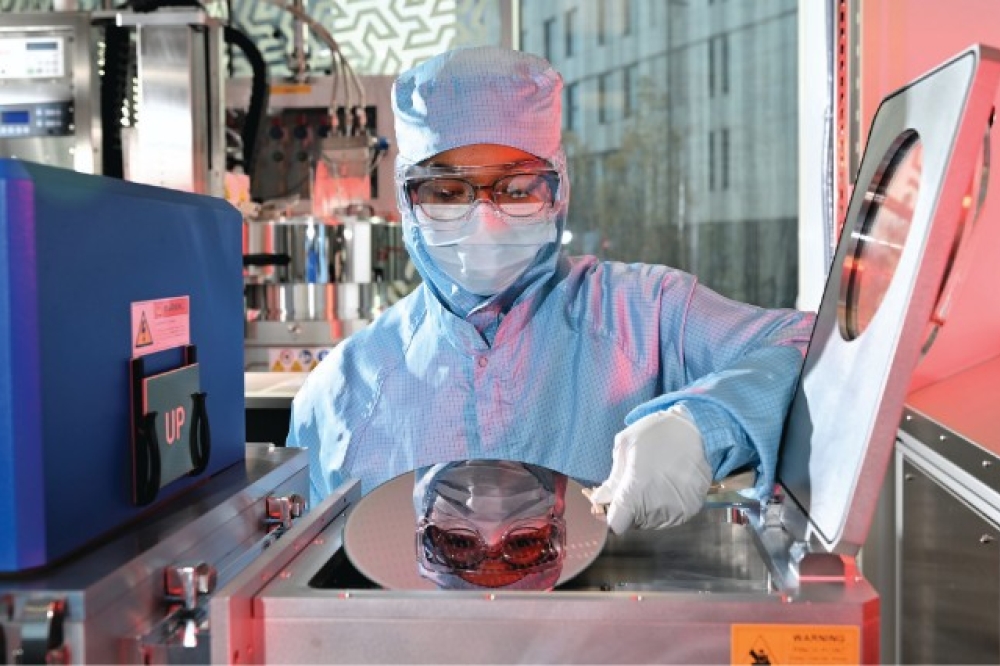
The CORNERSTONE foundry at the University of Southampton offers both academic and industrial users a flexible solution for fabricating silicon photonics devices, as well as broader start-up support to accelerate the commercialisation of the technology.
An interview with Graham Reed, Professor of Silicon Photonics and Director of the Optoelectronics Research Centre at the University of Southampton, and Laura Hiscott, contributor at PIC Magazine.
LH: How was CORNERSTONE established and what role does it play in the UK semiconductor industry?
GR: We started CORNERSTONE in 2014 based on a grant from the Engineering and Physical Sciences Research Council (EPSRC). The reason was twofold; it was an additional income stream to the university to underpin the cleanroom, but also, because we have such a good cleanroom, we thought it would make sense to open it up to other academics in the UK. So the target audience was UK academic researchers who could use the CORNERSTONE facilities to fabricate their silicon photonics devices. That’s where we began. Now we started and always have been open source, which means we don’t encumber the intellectual property of the users. We don’t lock them in. We offer as much flexibility as we reasonably can. And along the way we’ve offered training in an ad hoc, unofficial way, because we often had users who were not specialised in photonics. For example, we had somebody who specialised in micro-electro-mechanical systems (MEMS), who wanted to marry MEMS and photonics together, so we trained them in photonics.
Over the years, the word spread without us advertising it much, so we gradually started to get more industry users. Last year, we had more industry users than academic and part of the reason for that is this open-source approach and flexibility. You can’t necessarily get the same platforms everywhere. Start-ups also want to be as far enough along their prototyping journey as possible in order to make an informed decision about how to go to a scale-up foundry. So small companies in particular started to use CORNERSTONE more.
As we became aware of that, we started to try and give these customers more of what they wanted. When we were going to offer this just to academics, we weren’t even thinking we would have a PDK, but industry-oriented users wanted a PDK, so we now offer that in all our platforms.
We still have academic users. They often have ideas about wanting to start a company, but don’t have funding yet. But equally, there are academics who just want to do their research, so they might use a Multi Project wafer ( MPW), or even use an MPW once and then do a bespoke run where they’ve put the funding on their grants because they want to demonstrate certain device ideas.
As silicon photonics has grown, the users have asked for more diverse platforms, so silicon nitride and then platforms for longer wavelength applications. Finally, we now offer a lithography service. That’s partly because we are in this unique position of having the only deep UV scanner in UK academia, as well as exceptional new e-beam facilities.
So a variety of groups are using us, even some of the bigger companies and sometimes defence-related people. We have quite a few international users as well; at the last count, we had customers in 24 different countries. And we were also invited into EUROPRACTICE, which is a big European brokerage where you can find people like TSMC and imec, so people could use us via that route.
LH: How does CORNERSTONE meet the differing needs of its various users?
GR: The needs of the users change with time. Something we’ve committed to in recent grants is that we will try to give the community what it wants. So we’ve added platforms because the community wanted them, and in the future they will want other things. When we were leading up to the last grant application they told us they wanted what we’re calling an online portal, a one-stop shop for silicon photonics in the UK, if you like.
So people could put their contact details on it and use it to find collaborators, partners, training etc. We haven’t started that yet, but it’s something we plan to do within the programme, and it’s the philosophy of trying to give the
community what it’s asking for.
LH: Which application areas do you think will gain the most traction with the platforms you offer?
GR: That’s a very interesting question, because if I was asked that 30 years ago, I probably would have got it completely wrong in terms of what happened. When we started doing this, we were thinking about sensor interrogation systems, not about high-speed communications at all. But it quite quickly changed. The big success of silicon photonics so far commercially has been a few companies leading the way in datacentre-based communications, and gradually silicon photonics has taken more of the market share.
Thinking of where the UK could benefit, you might think that communications might not be the biggest opportunity, because it already has big multinational leading players – the Nvidias of this world, Intel, Cisco, for example. However, the advent of co-packaged optics means there’s a whole semi revolution happening again to the communications infrastructure, the optical input/output demands and so on.
Things will probably evolve quite a lot, especially with the demands of AI and the linkage of AI chips with photonics chips. So that whole area probably has a new lease of life itself.
But then you have the emerging applications, like imaging, LiDAR, healthcare, defence, environmental sensing, and quantum. My view is that’s where the biggest opportunities for the small companies in the UK are, because they don’t have the corresponding dominant multinationals that they have to displace. But communications has a big lead, because it’s already essentially a commercial industry versus these emerging applications. It’s a really exciting time. There’s plenty of stuff going on. I wouldn’t want to bet my house on any individual application at the moment.
LH: CORNERSTONE focuses on silicon photonics, but this platform has traditionally had challenges with active components. Is the foundry exploring hybrid and heterogeneous integration?
GR: Yes, we’re looking at multiple different materials to integrate with silicon. Part of this is driven by people saying that silicon modulators are running out of steam. My view is there will be an all-silicon modulator-based solution to 400Gb/s per wavelength, which is the next industry milestone, maybe a year to 18 months away. Maybe after that the other materials will play a bigger role. But a lot of people would disagree with that and say that you need those other materials. The reason I don’t say that is because we’ve already done 200GBaud in an all-silicon solution, which isn’t yet 400Gb/s, but it implies that it might be possible. We’ve already done more than 300Gb/s in a PAM-4 format, and it’s not as much of a leap as it used to be to reach 400Gb/s per wavelength. In fact there are some solutions at 400Gb/s per wavelength out there, but they also include significant Digital Signal Processing (DSP), which is very power hungry, and we have been taking the approach of minimising DSP to ensure low power.
At one point speed was the only thing that mattered. Then, once we got to 50Gb/s in about 2011, people started to think that getting the energy consumption down is more important. Then it became speed again, because of increasing data demands. Now there seems to be less emphasis on energy than there was even two years ago.
However, a lot of people are working on ring resonator-based modulators, partly because they are inherently lower energy than the Mach Zehnder modulators. But they come with other problems; at an ambient temperature, they would drift, so you either put some sort of feedback loop on or you control the temperature, and both of those things require additional energy. That’s not to say you can’t do that, but it’s a question of the best trade-offs of speed and energy. There is a type of ring resonator where we also hold a world record for data rate. But equally, there are many types of ring resonator as well.
The other thing you could do to control ring resonators is something called optical trimming. When you use silicon to make a resonant structure, because it’s a high-refractive-index material, it will drift more than a low-refractive index material for a given temperature change. Secondly, it’s also more susceptible to fabrication errors. So if your waveguide is a little bit too narrow or wide (say), it won’t perform at quite the targeted resonant wavelength as it would if it was spot on accurate. Those sorts of variations are even observable in 12-inch wafer fabrication at the state of the art facilities.
Therefore, some people are looking at trimming, where you correct the manufacturing defects. It doesn’t change the drift with temperature. But imagine you’re trying to hit a resonant wavelength here, and you manufacture it, and your resonant wavelength is actually over there, if you only rely on thermal control, you’ve got to bring it all the way back over here first before you stabilise it. And that means that you use a lot more energy. If I can find a way of trimming it back to here, I’ve only then got to use the energy to keep it there. I haven’t got to use the energy to actually tune it there in the first place. So we also have a unique, non-volatile way of trimming that’s come out of our research group. That’s actually quite interesting for ring-based modulators too. So we’ll see which way these things end up going.
Finally, some of the folks who are using ring resonators to deal with the low energy aspect have discovered that they have to use digital signal processing to actually retrieve the signals, which is very power hungry. With the Mach Zehnder-based modulators, you are sometimes less likely to have to do DSP. Hence there is yet another trade-off. There are so many trade-offs that you have to consider what will end up being the winning technology. I think the jury’s probably still out in many ways.
Graham Reed, Professor of Silicon Photonics and Director of the Optoelectronics Research Centre at the University of Southampton
LH: Last year, CORNERSTONE won funding from the UK government. How is the foundry planning to use it?
GR: Up to now, CORNERSTONE has literally just been a foundry, and we’ve been making things for other people based on their designs. But as I mentioned, we’ve tried to be flexible along the way and do a little bit of ad hoc training to help the start-ups with whatever they’re trying to do. So when we heard this call was coming, we asked: could we put more of a UK infrastructure spin on this, and bring in other partners from around the UK to deliver some of these things in a more structured way?
For example, thinking about start up support, we are working with the Future Worlds accelerator, and there’s another accelerator from Silicon Catalyst involved who run the ChipStart programme. So that means that we have people who do accelerator support for a living, rather than us trying to do it in an ad-hoc way.
We’ve got STFC who do electronics training. We can do some of the photonics training, and Glasgow are a part of this too, but it’s better to have a specialist doing the electronics training, because pretty much for every PIC you have, you’ve usually got an electronics chip to interface to the real world. Therefore, STFC have become a partner to do some of that training for the photonics people.
I mentioned earlier the portal and that extends to networking. We’re doing a lot more engagement with government and policy work. There are people employed on the CORNERSTONE grant who are embedded in our policy unit at Southampton who are engaging with government as part of the programme. All these activities are things we wouldn’t have done before as a foundry, and the overarching aim is to speed up the journey of a start-up.
We’ve already seen some of our start-ups getting funding. Obviously, we can’t take credit for that, but I would hope that we’ve accelerated their journey. The core of this is still the foundry doing what it does, but now we’ve got people who can also support start-ups in the other ways, who will have better contacts and better pathways already established that we can effectively take advantage of.
LH: Last year, CORNERSTONE announced it would be taking part in PIXEurope. Could you tell me about the foundry’s role in that project?
GR: It’s an interesting story. The PIXEurope consortium was already formed and had been in place for the best part of two years, before the UK was once again eligible for European funding. They knew how much money was available in the call and they had allocated it to participants.
We knew a lot of the partners from previous collaborations and they were very supportive of us being involved on a technical level, but there wasn’t money to give us because they had allocated it already. If they’d given us money, they would have had to take it away from somebody else who’d been contributing for two years.But it was important for us to get in, because it’s a five-year funded programme, followed by five years where it’s self-sustaining. Therefore, if the UK was not involved, it would have been outside of this programme for 10 years, which would have been really detrimental to the UK photonics landscape.
Now, whatever you get from that programme, there has to be matching funding from the home country. We asked DSIT if they could, on this one occasion, give us the equivalent of the matching funding, even though we wouldn’t get any from PIXEurope. The consortium said, if they did that, they would let us in. But DSIT said we can’t do that, because it would set a precedent. They suggested that we try and persuade Europe to increase the amount of funding, because the UK is paying into Europe now but we’re not always able to get our equivalent share back out. So we were doing the technical bit with the consortium, and DSIT was doing the politics. They did a fantastic job, and persuaded Europe to
change the budget.
At that point, we had to offer the consortium something they didn’t already have. We combined with Cambridge, who we’re already working with, because they are one of the leaders in graphene.
There’s a lot of background work on photonic applications of graphene, and Cambridge were particularly keen to put graphene-based photonic devices onto silicon photonics. So we jointly went to the consortium and said: you don’t have this. Would that be something you would want? And they said yes.
Now that the funding has been approved, I’m hopeful that we will do more than just the graphene, because I think we have a lot more to offer now. We don’t want to displace other partners, because we’re all working as a team, but I think there will be things that we can do that other partners cannot, perhaps in some of the emerging, longer-wavelength platforms, for example. We’re saying to the consortium: everything that CORNERSTONE can do is available to you if you want it. It’s very early days for that programme, but importantly for the UK we’re in.
LH: As the industry continues to evolve, how do you see CORNERSTONE’s role evolving with it?
GR: I would like to see silicon photonics evolve in such a way that the UK benefits from it. We started the silicon photonics group in 1989. There was a little bit of work in the US, theoretical work from about 1986, but there wasn’t very much practical work at all. So we were more or less in at the very beginning of silicon photonics. So I personally would be very pleased to see the UK benefitting from it.
We are getting feedback from commercial users, and small companies in particular, that they need a flexible prototyping silicon photonics foundry for several reasons. Firstly, they may not be able to get into a commercial foundry, because at the early stages they won’t have the volume. Secondly, they might not want to get into a commercial foundry too soon, because it might encumber their IP. And thirdly, they might not know which commercial foundry to get into, because they’re not far enough along the prototyping journey to know which foundry suits their technology best.
Therefore, I think what the UK needs is that type of flexible prototyping service. Now it doesn’t have to be CORNERSTONE. We can separate the questions of whether we need one, and where or how it might be implemented. Even if it wasn’t CORNERSTONE, it’s better for the UK if there is such a service for start-ups and companies. But if that decision was taken, then CORNERSTONE might be in a good position to bid for that and offer a solution.
The motivation is that the UK does better out of silicon photonics than it will do otherwise, because, like many technologies, I think there’s a real danger that this gets exploited all around the world and everywhere but the UK, even though we pioneered the technology.
LH: In theory, silicon photonics could be scaled up and become very cheap, like traditional electronic semiconductors, but we haven’t reached that point yet. What are the barriers for silicon photonics companies in going to higher volumes?
GR: For years people have talked about whether datacentre communications is a high-volume application or not. There is a growing number of datacentres, and they need increasing numbers of transceivers so it’s obviously growing. But in terms of consumer products, it’s not high volume, because it’s very specialised and specific.
If you think about autonomous vehicles, there are already driverless taxis in some cities, and they’re based in part on LiDAR. They’ve got big rotating things on the roof because
it’s a mechanical system. Now you can implement LiDAR imaging via PICs, so instead of the system on the roof, you could deploy chips around your vehicle to give you the same, or in fact probably better, sensing as part of the driverless vehicle control system.
In terms of round figures, let’s say you have 10 chips per vehicle. Most people have a vehicle, lots of people have two. That’s a proper mass-market application.
In healthcare, if you had a chip that does cancer detection, you might be able to do it at home or at the doctor’s surgery. You’d definitely have it on the wards of hospitals. That’s potentially another mass market. And there are so many healthcare applications that you could probably measure multiple measurands with the same chip. That’s going to be much higher volumes potentially.
It’s a bit of a chicken and egg. For many years people were asking: what’s going to be the really high-volume silicon photonics application? But datacentre communication has progressed so far now that I think everyone believes this is a commercially viable technology. Otherwise you wouldn’t be seeing the proposals and implementation of co-packaged optics.
But by the same token, it gives confidence to emerging applications that the technology works and is viable. There are differences obviously, but it’s no longer such a massive leap of faith that mass-market applications can be implemented in silicon photonics.
LH: What advice would you give to researchers and start-ups working on integrated photonics?
GR: Well obviously I would say do silicon photonics! But assuming they’re already doing that, I would say aim high and be ambitious. If I look back to when I started doing silicon photonics, did I ever think we would get anywhere near 400G?
Not a chance, and I don’t think anybody did. And even if I did think we could do it, I would have expected there would be competing technologies that would probably do it better. But as it turns out, silicon photonics performs much better than most of us expected. It depends on what your ambition is.
If you want to be an entrepreneur, the funding is much more likely to be available now, because the technology is now much more commercial. If you want to be a researcher, there are way more jobs available in research, in large and small companies, as well as universities.
You can work in areas of silicon photonics that interest you. In some ways I’m quite jealous of the new silicon photonics graduates these days, because they’ve got so much choice and opportunity. So aim high, change the world – because you can – but do something you’re motivated by.

Graham Reed, Professor of Silicon Photonics and Director of the Optoelectronics Research Centre at the University of Southampton