Technical Insight
Beyond silicon: building a photonic foundation for next-gen computing

AI, quantum, and high-performance computing are outpacing the limits of traditional silicon photonics. Hybrid organic electro-optic technology offers a new foundation – one that combines manufacturability with breakthrough performance and efficiency.
BY BRAD BOOTH, CEO, NLM PHOTONICS
Every leap forward in computing eventually runs headlong into a wall. For today’s AI workloads, that wall isn’t just compute, but also the energy required to move data. Inside hyperscale datacentres, photonic interconnects can account for 20–40 percent of total facility power consumption. As per-lane speeds climb past 200G, the question is not just whether we can move the bits, but also whether we can afford the watts to do so.
Traditional silicon photonics modulators work by shuttling charge carriers in and out of a waveguide to shift its refractive index. It’s simple and CMOS-friendly, but it comes at a price: higher capacitance, higher drive voltages, and degraded signal integrity as speeds rise.
The consequence is a hard limit; whereas electronics developed for a long time according to Moore’s Law, photonics does not have a similar rule. Devices get bigger instead of smaller as you push performance, consuming more power and wafer real estate and generating more heat that must be removed from the system. It’s the wrong direction for an industry that needs to pack more bandwidth into tighter envelopes while cutting energy per bit.
Traditional silicon photonics modulators have carried the industry impressively far, serving brilliantly for 100G and 200G, while offering manufacturability that has allowed the photonics industry to build on a foundation of familiar fabs and processes. But physics, unfortunately, is unforgiving. At higher baud rates, the power penalties pile up, the signal quality declines, and silicon photonics’ viability faces a cliff edge. Beyond 200G per wavelength, these issues can’t be sidestepped by clever design alone.
Facing relentless bandwidth demand, but finite power budgets, many companies are seeking to avoid the current unsustainable trajectory by investigating alternative photonic platforms. The new high-bandwidth platforms being explored rely on the Pockels effect, which permits a lower electric field to modulate light very efficiently. It’s a subtle difference with enormous impact for achieving higher bandwidths and reducing power consumption.
Currently, researchers are pursuing two material approaches for new modulators: inorganic materials like lithium niobate or barium titanate, and organic materials like polymers, organic small molecules (monomers), or liquid crystals. Organic materials are introduced into the silicon photonics platform to provide high-performance modulation, replacing traditional p-n junction-based modulators. But not all Pockels-effect materials are created equal, especially as industry demands for performance, loss, manufacturability, reliability, size, and efficiency become more important.
Organic electro-optic (OEO) materials have emerged as a strong contender thanks to their ability to integrate with traditional silicon photonic manufacturing. This combination creates silicon organic hybrid (SOH) modulators, in which the p-n junction is replaced with a slot waveguide containing an OEO material, providing a > 10x improvement in modulation efficiency. This permits SOH modulators to become more energy efficient and dramatically smaller. Drive voltages plummet and bandwidth climbs. Thermal stability – once a stumbling block for organic materials – has also made advancements to levels compatible with commercial photonics manufacturing.
Crucially, the SOH approach is fab-friendly. The organic material is deposited in a post-fabrication process module without disrupting established front-end-of-line silicon photonics manufacturing flows. For foundries, that means no modification to their traditional manufacturing or to their tooling. The post-processing step can either be part of a back-end-of-line step for a foundry or a pre-processing step for an outsourced semiconductor assembly and test (OSAT) firm.

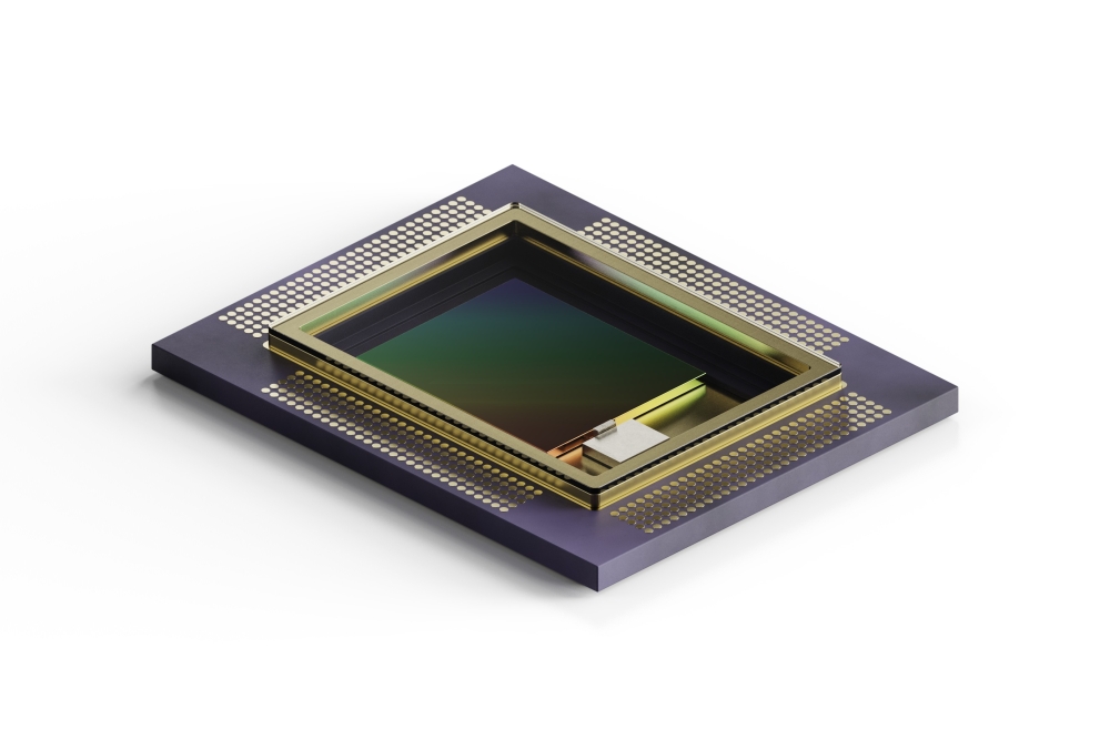
Generations of OEO materials, adapted from Dalton et. Al. 2023
Productization
Designing OEO materials is not just about chasing the highest electro-optic (EO) coefficient. It’s about balancing competing factors including wavelength of operation, responsivity, and loss. Over the past two decades, chemists have steadily improved these trade-offs through improved theoretical understanding and computationally guided design. Early-generation OEO materials were repurposed dyes blended in common polymers. Now, with the current third generation of materials, methods including chromophore engineering, tuning of sidechains for processibility and stability, and advanced poling techniques have unlocked stability and activity levels that rival or exceed inorganic materials.
At NLM, we’ve focused on building tuneable material families. Selerion HTX, our first thermoset material, delivers EO coefficients of 150–450 picometres per Volt – between 5-15x that of lithium niobate. Additionally, Selerion-HTX showed for the first time that high-performance OEO materials could be crosslinked into a thermoset material with long-term stability at temperatures in excess of 120 degrees C. This combination of strong activity with exceptional thermal resilience makes HTX well-suited to pluggable optics and long-lived telecom infrastructure, where devices must survive high operating temperatures, field deployment, and extended shelf life without performance drift.
Our newest material, Selerion-BHX, crosses the 1000 picometres-per-Volt threshold while maintaining long-term stability at 85 degrees C. It now holds the record for modulation efficiency in a slot-waveguide device, with a modulation efficiency of 0.038 Volt millimetres at 1550 nm in a plasmonic organic hybrid (POH) modulator. Selerion-BHX’s record-breaking electro-optic activity enables ultra-compact modulators with very low drive voltages – ideal for co-packaged optics, optical I/O, and space-constrained systems like satellites, where footprint and energy savings are paramount.
Each material finds a careful balance of chemistry, stability, and manufacturability, allowing the different variants to be tailored to the needs of specific architectures and environments. One of the benefits of organic materials is that they can be readily modified and tuned to the performance of the application. With an intrinsic bandwidth capability in the tens of terahertz, there is a lot of performance headroom in the technology.
In a recent commercial milestone, data tests performed in collaboration with Keysight Technologies confirmed 224G PAM-4 (4-level pulse amplitude modulation) data transmission for an 8-channel silicon-organic hybrid PIC using Selerion-HTX. The tests demonstrated exceptionally low driver requirements: 0.31 Volt-millimetres on the best single channel, representing a 10-15x modulation efficiency improvement over traditional silicon photonics modulators.
These results represent real-world improvements in 200G performance and a path to 400G in a commercially available silicon photonics platform. While the rote understanding of organics in photonics was once “great on paper, unstable in practice”, the story has now changed, and productisation is well underway.

Testing performed in collaboration with Keysight demonstrating a 224G PAM-4 eye diagram on NLM’s 1.6T DR8 SOH PIC.
Impact
What does all of this mean for operators and system architects? When photonic links represent 20–40 percent of an AI datacentre’s power budget and SOH devices reduce link power by 20–50 percent, total site energy use can be reduced by up to 15 percent. This substantial reduction translates into the ability to add racks and expand AI capacity without building new facilities. It’s a path to sustainable growth in an era when grid availability is a significant gating factor. This means not only millions of dollars per year saved in energy costs, but also the option to defer construction of entirely new datacentres.
Any ability to rein in power consumption with each new generation of bandwidth requires photonic technology to be able to scale and eventually to be integrated tightly with the electronics. This tighter integration will introduce greater thermal challenges in operating environments and in manufacturing. But this is a challenge that NLM Photonics is focused on solving with new generations of OEO materials, to continue supporting datacentres far into the future.
While AI is the most visible driver of alternative electro-optic material development, the benefits of OEO materials ripple across numerous other domains too. Quantum computing systems, for instance, demand low-loss, high-responsivity links at cryogenic temperatures to maintain coherence of entangled states. Addressing this need, NLM Photonics has developed a material for a quantum customer’s specific requirements.
Meanwhile, in the space and satellite sector, size, weight, and power (SWaP) considerations dominate payload economics. A smaller, lighter, more energy-efficient modulator directly translates into more capacity or reduced launch costs. NLM’s Selerion family can meet these stringent SWaP constraints via either SOH or POH devices.
Another potential application of NLM’s products is in telecom infrastructure, where coherent links have become the standard. Selerion-HTX has lower-loss performance in the C- and L-band, while delivering the modulation efficiency required for low driver swings with clean signals.
Finally, NLM’s OEO materials permit the reduction of footprint and drive voltages, which are critical in chip-to-chip and co-packaged architectures, making them useful in optical I/O. For example, NLM’s 1.6T SOH PIC is 40 percent smaller than a traditional 1.6T silicon photonics PIC, and NLM’s 3.2T PIC is even smaller than the 1.6T PIC. SOH micro-rings can also be designed to be athermal, reducing thermal control needs.
Each of these domains underscores the same point: far from being just a “datacentre play,” stable, efficient OEO materials could become a foundational technology.
The road to adoption
When NLM Photonics launched in 2018, the idea of stable, scalable hybrid OEO modulators was still considered speculative. Seven years later, we’ve gone beyond supplying research materials to developing ecosystem partners, operational PICs, and our Selerion family – all driven by our R&D focus on next-generation materials, process technologies, and modulator designs.
We continue to collaborate with partners, including universities, start-ups, hyperscalers, and foundries, and publish peer-reviewed papers confirming record performance and
reliability. The progress has been steady, deliberate, and measurable. The next frontier isn’t just higher bandwidth or lower voltage; it’s reliability and manufacturability at scale.
That means wafer-level processing – automating deposition, encapsulation, crosslinking, and poling so OEO can be added at the same scale as any other photonic step. It also means scaling from today’s 1.6T DR8 PICs to next-generation devices capable of 3.2T and beyond, supporting 400G per lane and beyond.
For the technology to reach its full potential, we will need to work on application-specific tailoring, designing OEO materials optimised for highly technical and future-focused markets and applications. We will also need to continue our ecosystem collaboration, working with foundries, hyperscalers, and customers to ensure NLM’s materials, processes, and devices align with demand for energy-efficient communication.
Ultimately, the vision is a photonic ecosystem where organics coexist with any photonic platform to reap the benefits of efficiency and scalability as bandwidth pushes forward and new markets gain traction. Together, they can unlock the headroom needed for AI, quantum, and whatever comes next. As a small start-up, NLM Photonics’ approach is to enable partners in the photonics ecosystem to adopt OEO technology and provide the benefits to their customers. Currently, we are working with our partners on the development of a Selerion-HTX ink that can be easily used by foundries. We’re also working with our foundry partners to make the process technology and device designs available in their PDKs. Our goal is not to disrupt the existing supply chains, but rather to enhance them with higher-performance and lower-cost PICs.
As such, NLM Photonics’ technology is designed to fit seamlessly with existing photonic platforms. Our 1.6T DR8 PIC, fabricated at Advanced Micro Foundry, used a standard commercial process flow and the post-processing step was performed at our facility. Over time, the post-processing will be transferred to partners to enable high-volume
manufacturing.
We also engage with standards bodies, because interoperability and conformance are required for new technologies to succeed. Players in the photonics industry must feel that OEO fits into their existing ecosystems, from protocol to manufacturing to operational compliance. Our mission is to lower barriers to entry for our partners and their customers.
The rewards of OEO adoption can be profound: reduced power use in AI datacentres to support sustainable growth, enablement of quantum systems to scale using existing photonic platforms, and a communications future that can scale with the existing supply chain. Seven years of advancements in hybrid OEO development show that SOH modulators are the most viable path to 400G and beyond for datacentres, as well as an extremely promising foundation for a host of next-generation networking applications. The challenge ahead is scaling production, building trust, and integrating with the broader photonics ecosystem.

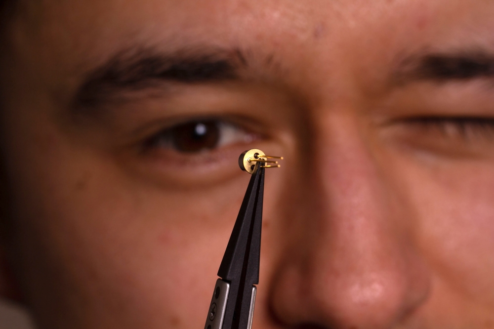
Dr. Scott Hammond, Senior Director of Process Technology of NLM Photonics, in the NLM Photonics clean room with the Company's wafer.