Consortium brings high-volume manufacturing tools, advanced packaging to Europe

APPLAUSE is an ECSEL Joint Undertaking project –which focuses on developing advanced packaging for photonics, optics and electronics for low cost manufacturing.
At the end of October a consortium of 31 European electronics packaging, optics and photonics key players, equipment suppliers and testing experts launched a new project, “Advanced packaging for photonics, optics and electronics for low cost manufacturing in Europe,” simply called APPLAUSE.
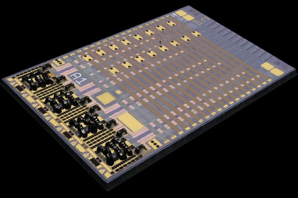
The project fosters the European semiconductor value chain by building new tools, methods and processes for high volume manufacturing. The 34M€ total budget for the three-year project is co-funded by Horizon 2020 and national funding agencies and industries, as a part of the Electronics Components and Systems for European Leadership Joint Undertaking (ECSEL JU).
The APPLAUSE project is coordinated by ICOS Vision Systems N.V. (Belgium), a division of KLA Corporation, and has partners from 11 countries, including 10 large enterprises, 11 small and medium-sized enterprises (SMEs) and 10 research and technology organisations. “APPLAUSE will focus on advanced optics, photonics and electronics packaging for multimodal sensing systems. High volume manufacturing is supported by a strong contribution from process and process control equipment R&D,” says Pieter Vandewalle, General Manager of ICOS, during the project’s kickoff meeting in Leuven, Belgium on May 21. “The technologies will be piloted in six use cases, each having an industrial end user,” adds Vandewalle.
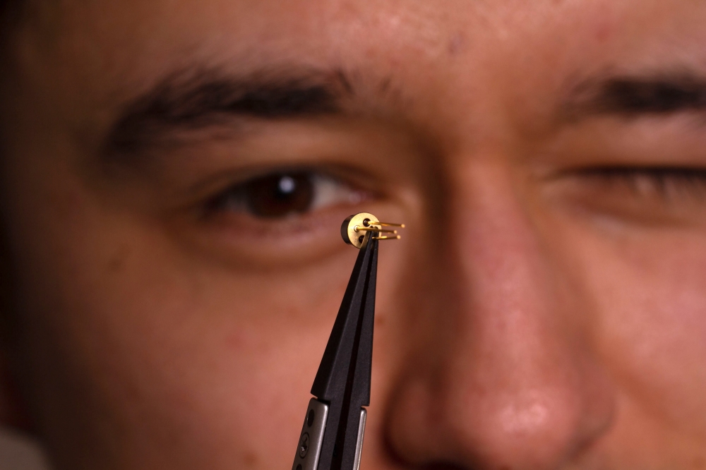
The six use cases include a substantially smaller 3D integrated ambient light sensor for mobile and wearable applications (ams AG, Austria); a high performance, low cost, uncooled thermal IR sensor for automotive and surveillance applications (IDEAS, Norway); high speed datacom transceivers with reduced manufacturing costs (DustPhotonics, Israel); a flexible cardiac monitoring patch (Precordior, Finland); miniaturized cardiac implants with advanced monitoring capabilities (Cardiaccs, Norway); and an optical water measurement module with cost-effective packaging of components (Vaisala, FinIand).
“This collaborative project builds the competitive edge of component and systems development in Europe. We develop new capabilities and demonstrate their match to the future needs of European industries. This accelerates the manufacturing uptake of the new technologies and shortens time-to-market” per Paula Pennanen, project manager at Spinverse.
The expected project impacts may include an increase in revenue for the project partners, exceeding 300M€, by 2025. The new technologies developed in the project have the potential for increased market share with additional access to new market segments for the industrial partners. The strategic, high level objectives of APPLAUSE include (1) developing new tools, methods, and processes for automated mass manufacturing and advanced packaging for the semiconductor, optics and photonics industries, (2) bringing advanced packaging and high volume manufacturing concepts to optics and photonics via six industrial use cases, and (3) increasing the competitiveness and global market share of European semiconductor industry, especially the manufacturing equipment, packaging and assembly industries.