Accelerating MEMS and Photonics Scaling

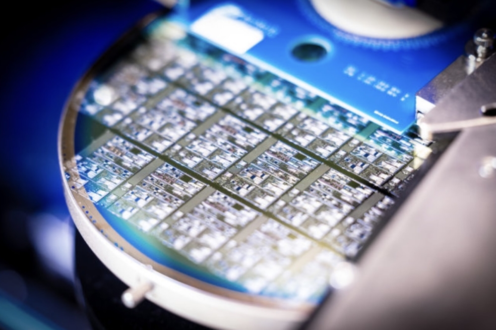
300‑mm wafer technology is accelerating MEMS and photonic IC scaling, unlocking higher yields, lower losses, and broader commercial adoption.
Advances in 300-mm wafer manufacturing are helping to close long-standing production gaps in MEMS and photonic integrated circuits (PICs), paving the way for broader commercial adoption and tighter integration with the semiconductor ecosystem.
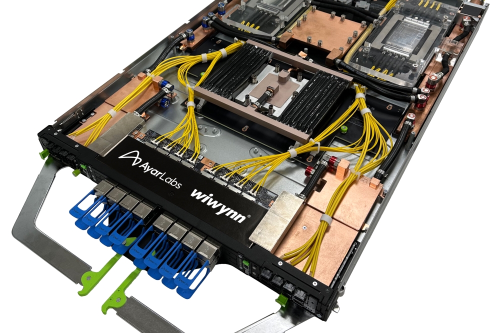
Over the past two decades, PICs and MEMS technologies have transitioned from research-focused development to product-driven engineering, with growing demand from AI, data centers, sensing, and communications markets.
As applications scale, the emphasis has shifted from proving device feasibility to delivering high-volume, semiconductor-grade manufacturing with consistent yield and reliability.
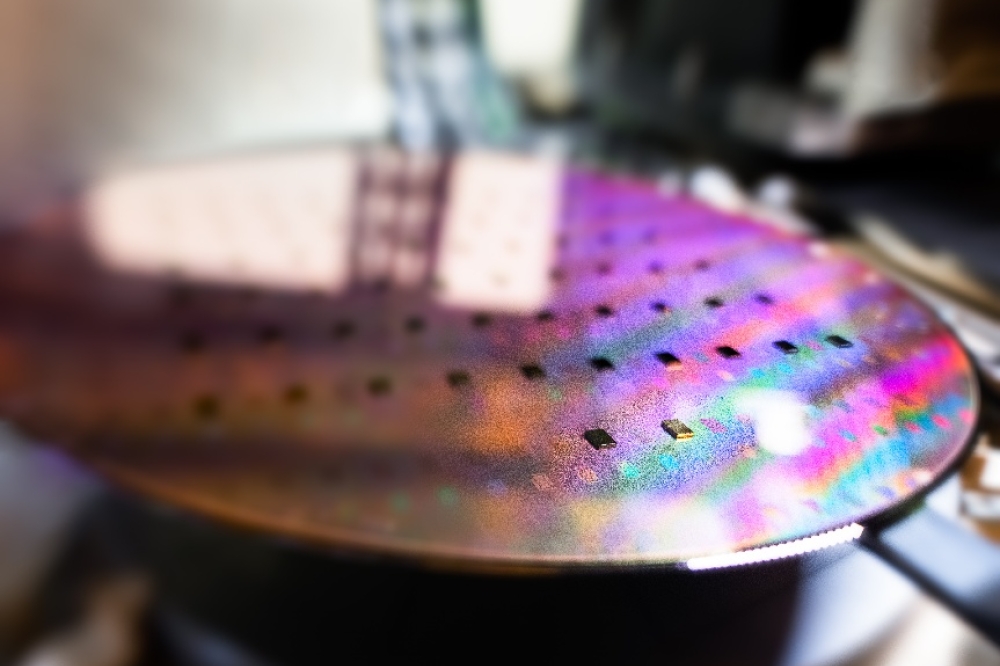
A key enabler of this transition is the move toward 300-mm wafer platforms. While logic and memory manufacturing standardised on 300-mm production years ago, much of the MEMS and photonics industry continues to rely on smaller wafers and legacy tools.
Access to advanced 300-mm equipment improves film uniformity, etch precision, and process control factors critical to reducing optical loss, managing mechanical stress, and improving yield.
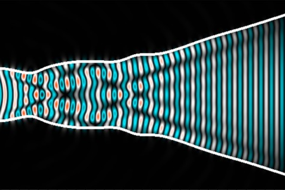
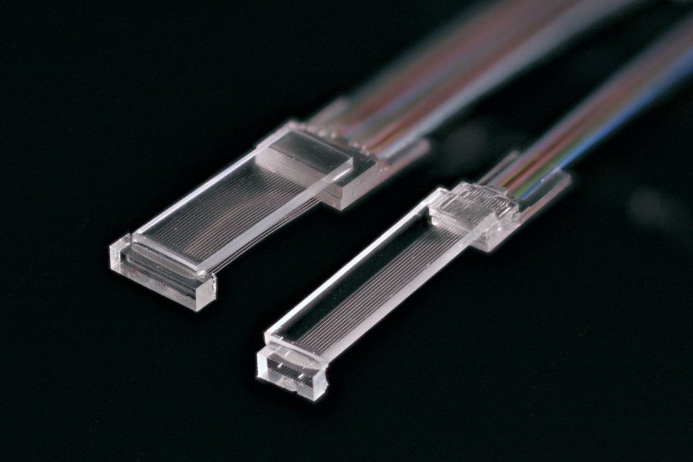
Both MEMS and photonics depend on high-quality thin films, precise etching, and advanced packaging.
Silicon nitride and oxide films underpin low-loss waveguides and MEMS structures alike, while increasingly complex etch processes must maintain tight dimensional and surface control across entire wafers.
Packaging remains another shared bottleneck, as optical alignment, wafer-level bonding, and thermal stability drive cost and scalability challenges.
Industry momentum is building around shared manufacturing platforms, particularly silicon-on-insulator substrates and wafer-level integration techniques.
As MEMS and photonics workflows continue to converge, improved process discipline and access to mature semiconductor infrastructure are expected to accelerate the path from prototype to high-volume production.
The shift toward scalable manufacturing marks a critical step in enabling the next generation of photonic and MEMS-based systems for sensing, communication, and computing.