Photon Design speeds TFLN simulation
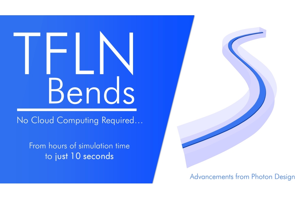
Native thin-film lithium niobate support in Photon Design's FIMPROP software enables rigorous waveguide bend simulations in around 10 seconds, helping accelerate the design of next-generation photonic integrated circuits.
Photon Design has announced native support for thin-film lithium niobate (TFLN) waveguide bend simulation in its FIMPROP photonic design software, enabling rigorous modelling of a benchmark 500 µm² 'S' bend in approximately 10 seconds using Eigen Mode Expansion (EME).
The company says the new capability delivers results comparable to finite-difference time-domain (FDTD) simulations while significantly reducing computation time.
According to Photon Design, the benchmark simulation was completed on a standard CPU-based laptop, whereas equivalent FDTD simulations can take more than an hour on a CPU or around 10 minutes using cloud-based GPU resources.
Unlike FDTD, which models the entire simulation volume, EME focuses on the propagating optical modes within the waveguide structure, making it particularly well suited to modelling adiabatic photonic components efficiently.
Thin-film lithium niobate is widely used for high-speed modulators in coherent communications, AI infrastructure and co-packaged optics, where designers often perform hundreds of simulation iterations during device optimisation.
"EME achieves its efficiency by modelling only the live material regions of the TFLN adiabatic bend, rather than the full bounding volume," said Dr Dominic Gallagher, CEO of Photon Design. "Since TFLN design is highly iterative, with engineers often running more than 100 simulations for each design, processing speed is a critical factor when choosing a simulation tool."