Inside Alcyon and Luceda’s collaboration to boost PIC manufacturing confidence
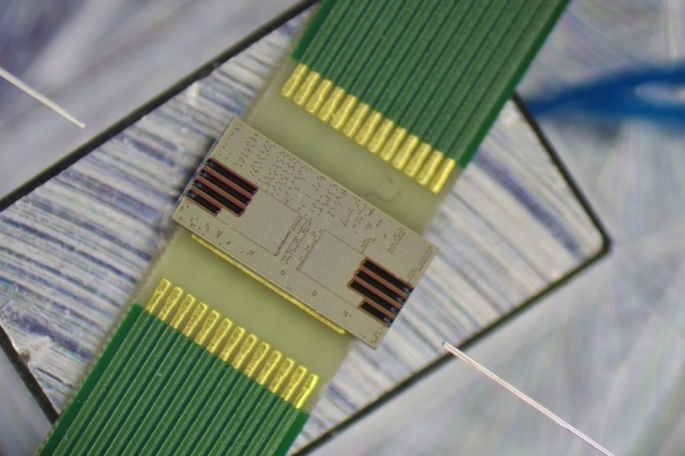
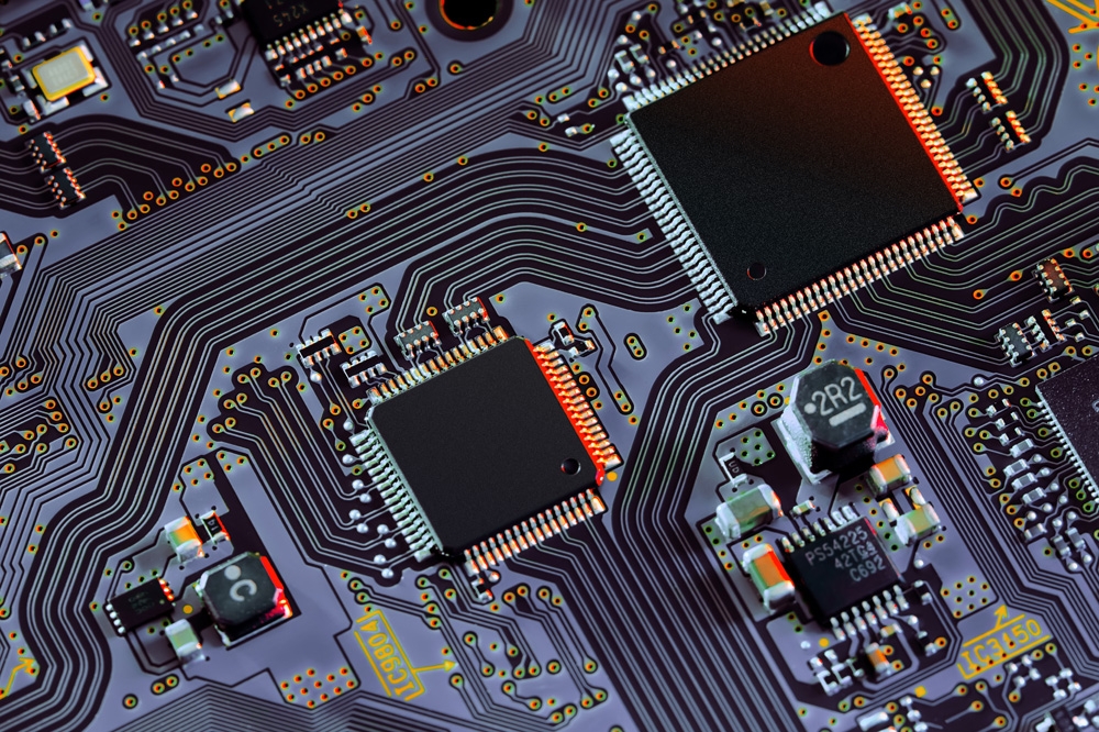
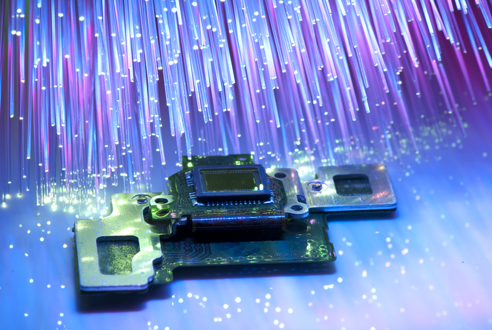
As photonic integrated circuits (PICs) gain traction in datacom, telecom, and quantum computing, scaling designs from the lab to high-volume manufacturing remains a major challenge. Minor variations in waveguides or component dimensions can dramatically impact performance, making yield and reliability key hurdles for designers. To address these challenges, Alcyon Photonics and Luceda Photonics have partnered, combining process-validated design IP with advanced variation-aware simulation tools.
Sarab Chopra, Editor at PIC Magazine spoke with Thibaut Bourguignon, PIC Team Leader at Alcyon Photonics, to explore why this collaboration is so timely and what it means for the future of PIC development.
SC: Why did Alcyon and Luceda decide to partner?
TB: The partnership really began in early 2024 when Alcyon was preparing to scale up for high-volume manufacturing. We were collaborating with major foundries like GlobalFoundries, Tower Semiconductor, and CompoundTek, and it quickly became clear that our internal design tools were no longer sufficient for the challenges of larger-scale production. Our internal tools were great for prototyping and smaller-scale work, but once you start talking about hundreds or thousands of chips, you need robust, commercial-grade software that can handle the complexity and variability inherent in high-volume production.
Luceda’s platform offered the kind of flexibility, compatibility, and advanced functionality that we needed. Beyond just software, it provided access to tools that allowed us to simulate designs more accurately, account for variations in the fabrication process, and ultimately ensure that our designs could be reliably reproduced across multiple foundries. For a start-up like Alcyon, this was a huge advantage. The partnership provides us not only with software but also with expertise and guidance, enabling us to accelerate development cycles, increase efficiency, and maintain high performance as we scale up production. It was a natural fit that aligned with both our technical needs and our strategic goals.
SC: How does combining your tools improve PH18 PIC yield and reliability?
TB: PICs are more complex than many people realise; they behave very much like analogue electronics, where tiny variations can have significant consequences. Even small differences in waveguide dimensions or delays between components can impact the overall performance of the chip. Traditional corner-based simulation approaches, which assume idealised extremes, just aren’t enough anymore. They fail to capture the full spectrum of variability that occurs in real-world fabrication.
By combining our process-validated passive component library developed specifically for Tower Semiconductor’s PH18 silicon photonics platform with Luceda’s spatially correlated variation simulation tools, we can now model and predict how these variations will impact yield and performance. Designers can optimise their layouts ahead of tape-out, reducing costly errors and improving the reliability of the final chips.
This approach essentially bridges the gap between simulation and reality. Instead of hoping a design will work once fabricated, engineers now have the ability to foresee potential yield issues and mitigate them proactively. The combination of our thoroughly verified components with Luceda’s simulation environment gives engineers both confidence and control. It’s about creating a workflow that is predictable, repeatable, and scalable so designers spend less time troubleshooting and more time innovating.
SC: What manufacturing challenges does this collaboration address?
TB: The biggest challenge in scaling PICs to high-volume manufacturing is variability. Small deviations, whether in waveguide width, phase delays, or other process parameters, accumulate across the chip and across production batches, causing performance inconsistencies and reducing yield. In traditional design workflows, engineers often don’t have the visibility to anticipate these variations until fabrication, which leads to multiple redesigns, wasted time, and increased costs.
Our collaboration addresses this challenge directly. By providing pre-validated building blocks and advanced simulation tools, we enable designers to account for real-world process variations from the very beginning. It allows them to optimise their designs not just for performance but for manufacturability and yield. This reduces risk, accelerates development cycles, and ultimately results in more reliable chips that can be confidently deployed in production environments.
For us at Alcyon, this is especially important. We can’t afford to waste time on iterations or face unexpected yield losses. Working with Luceda allows us to leverage their software and expertise to fine-tune designs efficiently, so we can scale production while maintaining high quality. It’s about combining the right IP with the right tools to meet the stringent requirements of modern photonic manufacturing.
SC: Which applications benefit most from this approach?
TB: Essentially, any application that relies on precise, repeatable photonic performance benefits from this partnership. Datacom and telecom are obvious examples where high-bandwidth, low-latency optical interconnects need to function flawlessly at scale. Quantum computing and other high-performance computing applications also gain from having predictable, reliable PICs, where even minor variations can have significant consequences.
But it’s not just about performance it’s about efficiency and time-to-market. By providing designers with verified, process-aware IP blocks, we reduce the need for iterative testing, shorten development cycles, and avoid costly re-spins. This approach enables companies to bring advanced photonic systems to market faster while maintaining the high reliability required in critical applications. It also opens the door for smaller companies to compete in areas that traditionally required large R&D budgets, because reliable building blocks allow them to focus on innovation rather than troubleshooting manufacturing issues.
SC: What does this say about the role of process-aware design IP?
TB: Process-aware design IP is absolutely critical in today’s photonics industry. Designers no longer want to start from scratch for every project; they want building blocks that are validated, verified, and reliable across different manufacturing platforms. With process-aware IP, you gain not only performance but also trust and efficiency.
At Alcyon, our goal is to provide IP blocks that are high-performing, thoroughly characterised, and ready for deployment across multiple foundries. By combining these blocks with variation-aware simulation from Luceda, we give engineers a complete toolkit to design robust, manufacturable PICs with predictable yield. It’s about reducing uncertainty, saving time, and creating confidence in the final product. In the long run, this approach helps elevate the entire ecosystem: designers, foundries, and end users benefit from more reliable, scalable photonic solutions.
SC: Looking ahead, what are your ambitions for this partnership?
TB: Our long-term ambition is to make our IP available in the libraries of the most common high-volume manufacturing foundries by 2027. That means any designer, anywhere, can access verified building blocks that meet rigorous performance and reliability standards.
Beyond that, this partnership is about creating a true synergy between our companies. Luceda helps us fine-tune our software and simulation workflows, while we contribute validated components and process knowledge. Together, we accelerate innovation, increase efficiency, and become more competitive in a rapidly evolving market. Ultimately, it’s about enabling reliable PICs at scale, reducing development risk, and empowering designers to focus on pushing the boundaries of photonics rather than worrying about whether their chips will actually work in production.