Lightmatter announces Passage M1000 3D photonic superchip

The company says its photonic interposer is the world’s fastest AI interconnect, enabling highest bandwidth and largest die complexes for next-generation AI infrastructure silicon designs
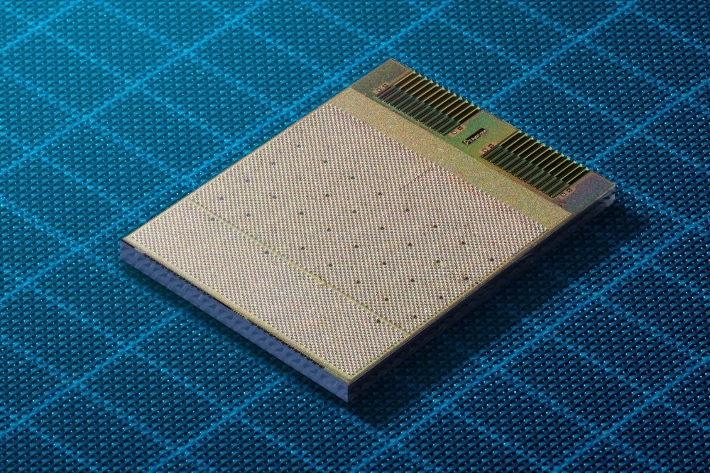
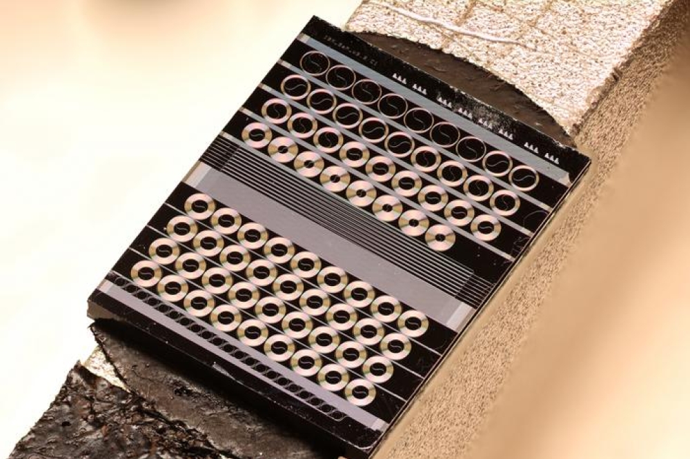
Photonic supercomputing company Lightmatter has announced Passage M1000, which it describes as a groundbreaking 3D photonic superchip designed for next-generation XPUs and switches. According to the company, the Passage M1000 enables a record-breaking 114 Tbps total optical bandwidth for the most demanding AI infrastructure applications. At more than 4,000 square millimetres, the M1000 reference platform is a multi-reticle active photonic interposer that enables the world’s largest die complexes in a 3D package, providing connectivity to thousands of GPUs in a single domain, Lightmatter adds.
In existing chip designs, interconnects for processors, memory, and I/O chiplets are bandwidth limited because electrical I/O connections are restricted to the edges of these chips. The Passage M1000 aims to overcome this limitation by unleashing electro-optical I/O virtually anywhere on its surface for the die complex stacked on top. Lightmatter says pervasive interposer connectivity is enabled by an extensive and reconfigurable waveguide network that carries high-bandwidth WDM optical signals throughout the M1000. With fully integrated fibre attachment supporting 256 fibres, the company says the M1000 delivers an order of magnitude higher bandwidth in a smaller package size compared to conventional co-packaged optics (CPO) and similar offerings.
Lightmatter has worked closely with industry leaders, including GlobalFoundries (GF) and Amkor, to facilitate production readiness for customer designs based on the M1000 reference platform, while ensuring the highest standards of quality and performance. The Passage M1000 utilises the GF Fotonix silicon photonics platform, which Lightmatter says offers seamless integration of photonic components with high-performance CMOS logic into a single die, creating a production-ready design that can scale effectively with AI demands.
“Passage M1000 is a breakthrough achievement in photonics and semiconductor packaging for AI infrastructure,” said Nick Harris, founder and CEO of Lightmatter. “We are delivering a cutting-edge photonics roadmap years ahead of industry projections. Shoreline is no longer a limitation for I/O. This is all made possible by our close co-engineering with leading foundry and assembly partners and our supply chain ecosystem.”
Thomas Caulfield, president and CEO of GF, said: “GF has a long-standing strategic partnership with Lightmatter to commercialise its breakthrough photonics technology for AI datacentres. The M1000 photonic interposer architecture, built on our GF Fotonix platform, sets the pace for photonics performance and will transform advanced AI chip design. Our advanced manufacturing capabilities and highly flexible, monolithic silicon photonics solution are instrumental in bringing this technology to market, and we look forward to continuing our close collaboration with Lightmatter.”
Vlad Kozlov, founder and CEO of LightCounting, commented: “The insatiable demand for scale-up bandwidth is fuelling interconnect innovation and momentum, with in-package optical integration at the forefront. Lightmatter’s unique 3D active photonic interposer presents a compelling advancement, with capabilities that surpass existing CPO solutions.”