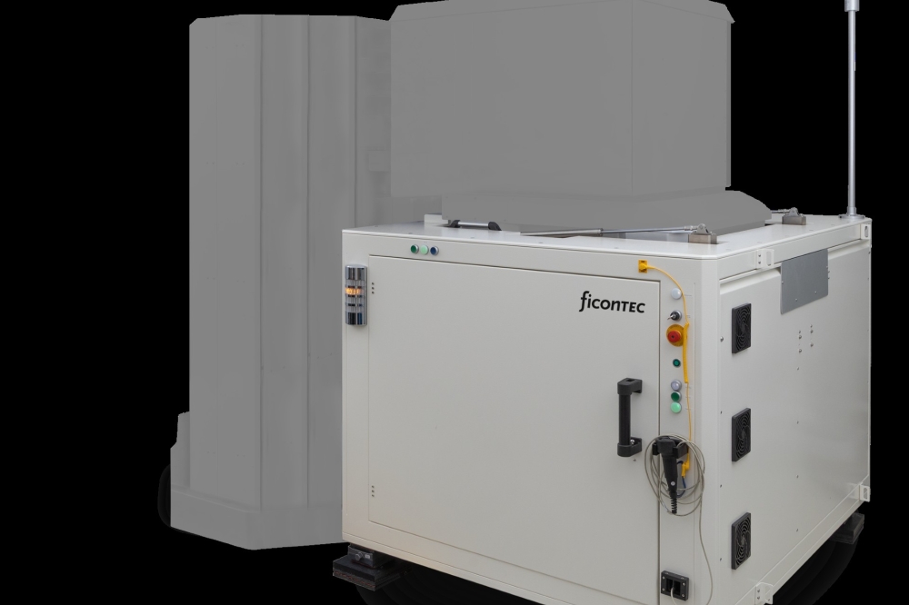
ficonTEC launches 300 mm double-sided electro-optical wafer tester
The new product, which the company describes as an industry first, is compatible with existing semiconductor ATE architectures and enables high-throughput, wafer-level testing of silicon PICs to support AI-driven computing demand
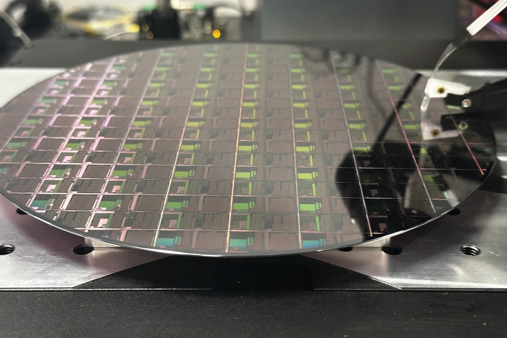
Automated assembly and testing machine company ficonTEC has launched its new 300 mm double-sided electro-optical wafer tester compatible with existing semiconductor ATE architectures, which it describes as an industry first. The new product is targeted at AI-driven silicon photonics computing demand.
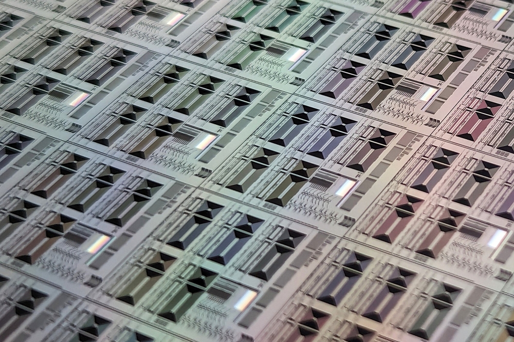
With immediate availability, the company says its new technology enables high-throughput, wafer-level testing of silicon PIC devices, which are at the heart of the co-packaged optics (CPO) enabled photonic engines featured in the highest-performance optical interconnects used within datacentres. By implementing broad compatibility with existing ATE architectures, ficonTEC says rapidly adoptable test capability is now commercially available for all major foundries facing the surging demand for contemporary and for recently announced next-generation CPO.
This new optical test cell directly docks with the ATE at a core software and hardware level, enabling DC and high-data-rate test capability on the top side and precision optical six-axis active alignment probing below. It also accommodates automatic wafer loading and incorporates a patented vacuum thermal control chuck assembly, in-situ fibre array calibration, end-face inspection, high-speed probe calibration, and automated PIC mapping.
According to ficonTEC, adoption is already in progress by a number of market-leading chip manufacturers and foundries, noting that the company’s intention here is to maintain a broad and open compatibility with all leading ATE manufacturers. Further near-term plans include developments for single-sided wafer formats as well as for die-level and module-level production test.
ficonTEC adds that its global sales & service network already serves around 1400 installed machine systems around the world, including a good proportion which have long contributed to the manufacture of high-end interconnect chiplets, and newer systems which support the CPO-enabled formats currently utilised in 400G, 800G, 1.6T interconnects and beyond. The company is currently expanding its support network – in particular in Taiwan, Korea, Israel, and the US – and aiming to boost its presence globally to effectively address the rapidly accelerating take-up of new technology in the AI computing sector.