X-FAB, SMART Photonics, and Epiphany Design partner on InP-on-silicon design
The specialty foundry, InP integrated photonics foundry, and design house are developing a collaborative platform combining InP chiplets with SOI technology via micro-transfer-printing for high-speed, energy-efficient optical transceivers
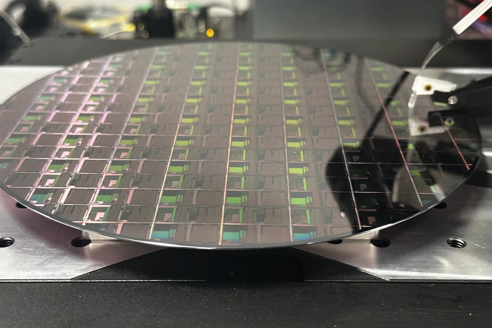
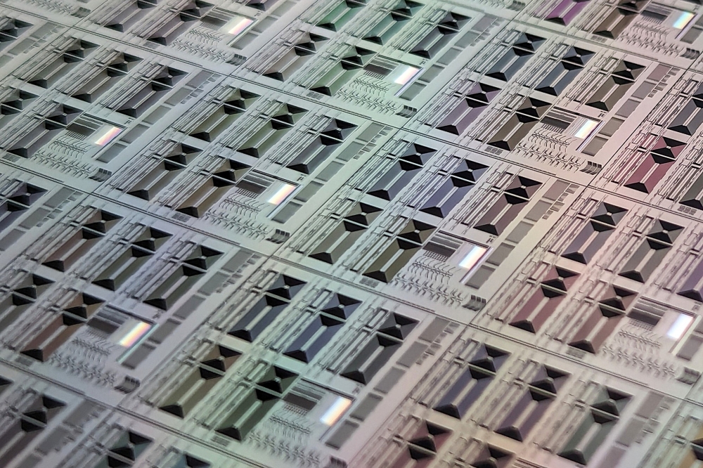
X-FAB Silicon Foundries SE, SMART Photonics, and Epiphany Design, are collaborating to develop a new heterogeneous photonics integration platform that combines the strengths of indium phosphide (InP) and silicon-on-insulator (SOI) technologies, enabling multi-terabit data rates for datacom and telecom applications.
Through the co-optimisation of SOI, InP, and micro-transfer-printing (MTP) technologies, the new platform aims to address customer requirements for high-speed data rates and energy efficiency in high-volume manufacturing of optical transceivers. The companies say it also enables new functionalities and improved system performance while reducing integration costs through relaxed photonics packaging requirements. MTP technology, developed by X-Celeprint, aims to provide a broad degree of freedom for the system and product designers, by allowing flexible integration of chiplets into the product design.
According to the companies, the collaboration has made significant progress, resulting in the development of a design flow and PDK that enables the design of photonic circuits integrating InP chiplets on an SOI platform. This design flow is implemented in Luceda's IPKISS EDA tool. Luceda's technical expertise and support enabled the design of the demonstrator.
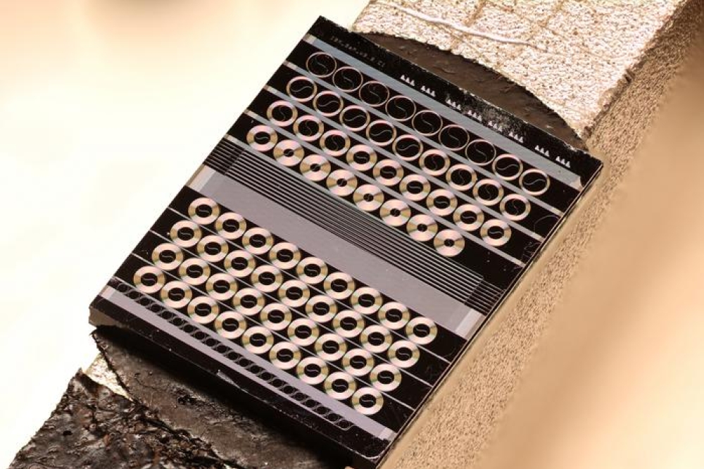
As part of this development, Epiphany Design – an X-FAB innovation and XCHAIN partner – has demonstrated the new heterogeneous InP-on-SOI design flow with an optical transceiver demonstrator. This collaboration will be showcased at the 50th Optical Fiber Communication Conference (OFC) in San Francisco.
“By bringing together the integration density of silicon with the high performance of InP actives, we enable new possibilities for disruptive innovation in telecom, datacom, and beyond,” said Jörn Epping, CEO of Epiphany Design. “This approach empowers PIC designers with greater flexibility and a clear path towards scalable, high-performance PIC-based solution.”
This collaboration builds upon the PhotonixFAB EU funding project, which supports the development of industrial pilot lines for silicon photonics SOI, MTP-ready InP chiplets and MTP of InP chiplets on SOI and silicon nitride photonics wafers.
X-FAB says the complete design flow will be available for early access in the first quarter of 2026, with a goal of supporting industrial prototyping for lead customers by mid-2026, with production ramp-up readiness in 2027.