Propelling PICs from idea to MVP in under 12 months

Light Trace Photonics has developed a cutting-edge pipeline for developing new integrated photonic products quickly and effectively, supporting companies with technical feasibility studies, proven component IP, and circuit-on-a-chip evaluation modules.
By Jake Biele, CEO, and Dominic A. Sulway, CTO, Light Trace Photonics
The world is entering a new era of technological innovation, where light is poised to revolutionise the way we compute, communicate, and sense our environment. PICs are at the forefront of this transformation, offering unparalleled speed, efficiency, and scalability compared to traditional electronic chips. Yet, despite their immense potential, bringing a photonic chip from concept to reality remains a complex, high-risk endeavour.
For start-ups and established companies alike, the road to a successful PIC product is fraught with challenges – lengthy design cycles, costly fabrication runs, and the need for deep interdisciplinary expertise. With a rapidly evolving ecosystem and a lack of standardised components and skilled engineers, even the most promising ideas can stall before reaching a functional prototype, let alone a fully-fledged product. The question remains: how can companies navigate these challenges and accelerate their time to market?
At Light Trace Photonics, we provide a solution. Our cutting-edge development pipeline is designed to take companies from initial concept to a minimum viable product (MVP) in under 12 months. Our approach is simple: minimise risk and maximise results during this early stage of product development.
By leveraging advanced proven photonic chip component IP, state-of-the-art design methodologies, and zero-barrier circuit-on-a-chip evaluation, we help our customers reduce risk, maximise results, and ultimately bring photonic innovations to life faster than ever before.

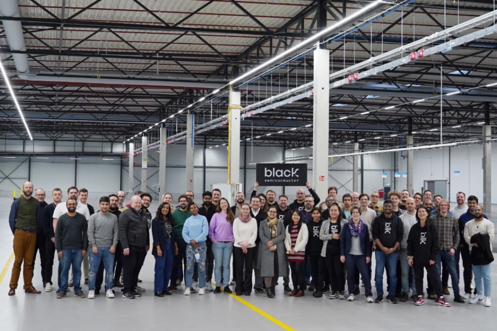
Figure 1. The Light Trace team: (l-r) Harry Alexander, James Blatcher,
Dominic Sulway, Quinn Palmer, Jake Biele, Steve Kitson, and Mike Ward.
Our pipeline supports companies through four key stages to MVP. First, we help customers establish a strong foundation through expert-led training and technical feasibility studies. Next, using proven component IP and expert guidance, we maximise the probability of achieving first-time-right circuit design. Then, we support clients to make confident decisions with rigorous post-fabrication in-house test and measurement. And finally, we accelerate early commercial success with a seamless, zero-barrier circuit-on-a-chip evaluation module, the LightPort:Pro.
We understand the challenges involved in this journey because we’ve faced and overcome them firsthand, during the development and launch of the LightPort – a cutting-edge module that enables engineers to get hands-on experience using and programming a PIC outside the lab (see Figure 2).

Figure 2. The LightPort training module helps upskill engineering teams.
The challenges: Why getting to MVP is so difficult
The world of integrated photonics is defined by extraordinary diversity – spanning multiple material platforms, wavelengths, and packaging options – standing in stark contrast to the more uniform landscape of microelectronics. This diversity is a testament to photonics’ vast potential and a formidable challenge. Unlike microelectronics, where established development pipelines provide a degree of standardisation, the rapid evolution of photonic technologies means that staying up to date with this evolving ecosystem is no small feat.
For companies developing PIC-based products, the challenge isn’t just understanding today’s capabilities – it’s anticipating what will become viable in the next two to five years. Choosing the right technology now requires foresight, as the wrong decision could leave a development eclipsed by emerging innovations before it even reaches the market. Navigating this dynamic ecosystem demands a strategic approach, one that balances near-term feasibility with long-term competitiveness, ensuring that today’s choices remain relevant among tomorrow’s advancements.
One area of particular interest is thin-film lithium niobate (TFLN), which has rapidly emerged as a potential frontrunner in next-generation photonics [1]. Long valued in bulk crystals for its exceptional electro-optic properties, lithium niobate waveguides have historically been constrained by fabrication challenges and limited integration with other platforms. However, the advent of thin-film processing is beginning to unlock its full potential, enabling ultra-high-speed modulators, low-loss waveguides, and compact, power-efficient photonic circuits.

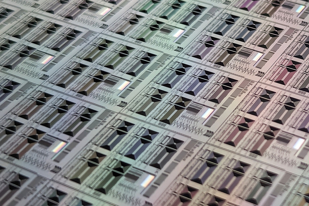
Figure 3. LightCraft’s proven component IP, made available via PDKs, will help you accelerate your product development.
With its combination of high bandwidth, low power consumption, and the establishment of commercial foundry offerings, TFLN is poised to play a transformative role in optical communications, quantum technologies, and microwave photonics. As fabrication techniques mature, and as these commercial foundries expand access, we see TFLN as a technology to watch – one that could redefine the landscape of integrated photonics in the coming years.
Besides this rapidly evolving and diverse ecosystem, another challenge that PIC entrepreneurs must navigate is a lack of access to proven IP. On this front, the PIC industry operates in a far less standardised environment than microelectronics. While increasing component density in photonics can enhance functionality and performance, it does not necessarily drive costs down in the same way as CMOS scaling. The analogue nature of many photonics circuits naturally results in a broader range of component types and designs to select from. In addition, photonic foundries often face pressure to customise processes for individual customers to improve component-level performance, leading to high R&D costs, lower yields, and manufacturing challenges.
This has resulted in an IP landscape that remains highly fragmented, with multiple companies reinventing fundamental components rather than leveraging standardised, proven building blocks. This limited standardisation makes component design selection a critical yet risky decision, as choices made early in development can have lasting consequences for manufacturability, scalability, and long-term competitiveness.
A third obstacle to overcome on the way to a successful integrated photonics product is the lengthy, costly fabrication processes involved. Bringing a PIC product to market typically requires multiple fabrication cycles, progressing from component-level validation to circuit integration and, ultimately, full system development. While early-stage development can leverage MPW (multi-project wafer) runs to reduce initial R&D costs, these still require significant investment – often tens of thousands of pounds per design – while iteration cycles average 5-8 months. Without a strong grasp of design best practices, many companies face repeated failed runs before achieving a functional prototype, significantly extending timelines and costs.

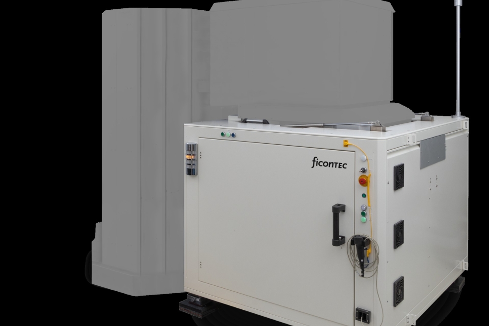
Figure 4. Automated die-level testing of components helps ensure informed decision making.
A critical challenge in early-stage circuit development is identifying and mitigating technical risks. While process design kits (PDKs) offer valuable design support, their effectiveness depends on a deep understanding of the underlying fabrication processes. Without this insight, even seemingly minor design choices can lead to costly setbacks on the road to product launch. Success in PIC development can hinge not only on leveraging standardised design tools but also on mastering the nuances of manufacturing constraints to ensure first-time-right fabrication.
Our solution: A streamlined pipeline for MVP success
Successful PIC development begins with a solid, up-to-date foundation of knowledge. At Light Trace, we bridge the skills gap with cutting-edge training and technical feasibility study services, ensuring in-house engineers gain the expertise needed to navigate the complexities of photonic integration. Our LightPort module is a game-changing tool designed to upskill engineers, demystify PIC technology, and align innovation with business objectives. Featuring a silicon nitride chip with a suite of programmable components – ranging from basic thermo-optic phase shifters through to complex wavelength demultiplexion schemes – the LightPort removes traditional barriers to hands-on learning, allowing all levels of engineer to experiment with photonic chips outside the lab.
In a rapidly evolving field, staying ahead requires both technical insight and strategic foresight. Our training programmes provide practical, hands-on experience while tailoring content to industry-specific challenges and applications. By equipping engineers with up-to-date knowledge and real-world design experience, we help de-risk development, accelerate innovation, and enable informed technology choices.
Once a team has a strong foundation in integrated photonics and a clear understanding of how it aligns with the company’s technology roadmap, the next critical step is to carry out technical feasibility studies to help roadmap development. This process is essential for ensuring the MVP maximises impact while laying the groundwork for future innovation and growth. At Light Trace, we work closely with engineers to craft a detailed, actionable plan that minimises risks, avoids costly detours, and accelerates the development timeline.

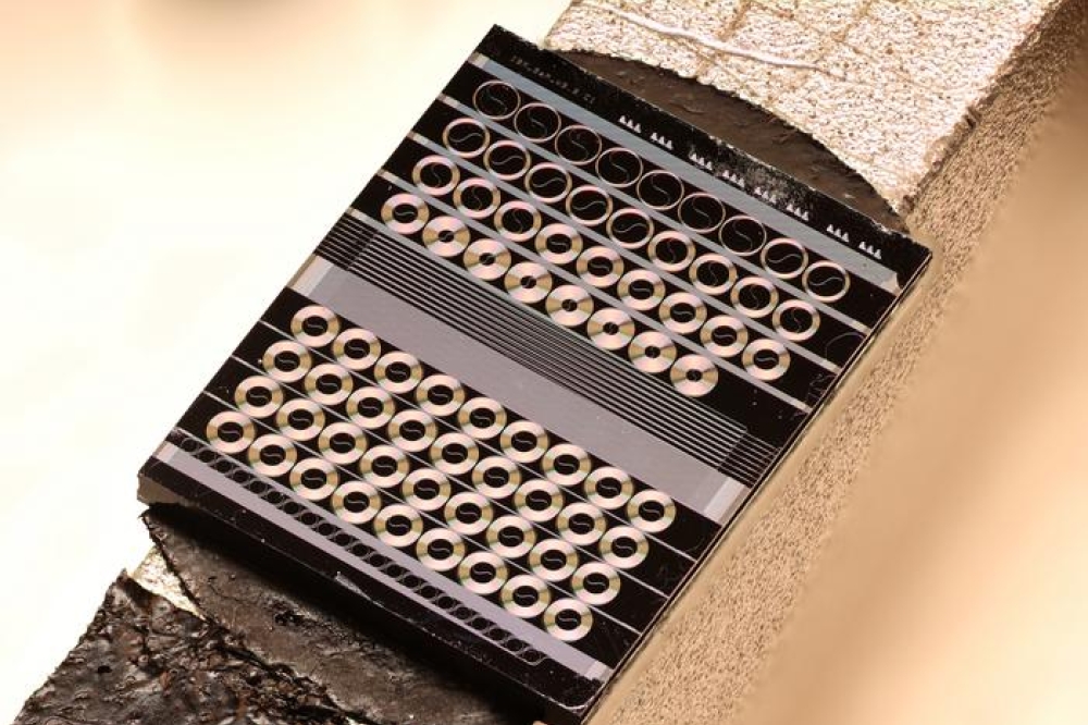
Figure 5.The LightPort: Pro packaging system makes demonstrating MVPs easier and more effective.
Key considerations include selecting the right platform and materials to ensure technological feasibility, financial viability, and scalability. We help define critical components and their specifications to increase confidence, performance, and reliability.
Our team also focuses on optimising packaging solutions to integrate photonic chips seamlessly into the wider product, factoring in cost projections, end market requirements, and volume production challenges. Finally, we assist with budgeting and timeline planning, ensuring that both the MVP and full-scale launch are achievable within set financial and time constraints. With our roadmap, innovators have a clear path forward, reducing uncertainty and driving their product to market with confidence.
With a clear roadmap in hand, the next phase is to design and fabricate a photonic chip that brings the MVP to life, minimising the number of fabrication runs needed to reach MVP. Achieving a first-time-right design requires precision, expertise, and access to proven IP, all of which help avoid budget overruns and development delays. While no MVP is flawless, it’s essential to identify the key value it must demonstrate to move to the next phase. Mapping this value to the technological risks in chip design and layout can be the crucial factor in determining success or failure at this stage.
Our LightCraft platform provides access to proven IP that has been rigorously tested in-house by the Light Trace team. This often allows our customers to bypass early design risks associated with key components and move quickly into circuit-level development. For teams without in-house chip design capabilities, LightCraft also offers expert support for system design and layout, ensuring that every aspect of the chip is optimised for success.
Key challenges in this phase include design optimisation for packaging – such as fibre I/O, laser integration, and thermal/electrical management – leveraging proven designs to minimise design risks and ensuring compliance with foundry processes. Our expertise extends to navigating supply chain relations to guarantee smooth transitions from design to fabrication.
Once the photonic chip is fabricated, the third stage involves testing, packaging, and demonstration. The goal here is to quickly and reliably assess component-level performance, enable engineers to evaluate circuit-level functionality, and demonstrate the MVP outside of a controlled lab environment to showcase its capabilities in real-world settings.
Component-level testing is crucial before moving on to circuit-level characterisation. Even if individual components have been proven in other fabrication runs, validating their performance within each new chip design helps uncover any potential fabrication errors and provides a solid foundation. At Light Trace, we’ve developed bespoke automated testing capabilities that efficiently generate performance reports for each component in the circuit, including DC and RF characterisation data, offering reliable insights and clarity as companies move forwards with integration.
This streamlined process ensures that our customers can assess and optimise the performance of both individual components and the overall circuit quickly, helping them demonstrate the MVP’s value and accelerate its deployment in the field.
After component-level performance has been validated, the next step is packaging and circuit characterisation. At Light Trace, we understand that our clients’ engineers, with their deep knowledge of their specific product lines, are most likely best equipped to carry out system-level characterisation. However, characterising a photonic chip at the circuit level can present new challenges related to electronic interfacing, optical interfacing, and temperature stability.
Unpackaged chips often require expensive, additional hardware for effective circuit interfacing, while custom software is often needed to programme and enable demonstrations. To simplify initial demonstration and chip interfacing, we integrate each customer’s chip circuit into the LightPort:Pro, a circuit-on-a-chip evaluation module we have developed to address these key challenges.
LightPort:Pro features up to 32 channels of optical fibre input/output to the chip, as well as up to 32 DC channels for programming it, with inbuilt 0-12 V precision voltage setting via interfacing with the Python programming language. Additionally, there are up to 8 GSG RF channels for applying/extracting signals to active components such as modulators and detectors, as well as 8 inbuilt (off-chip) photodiodes for easy debugging and live readout.
We use a Python-based scripting language for chip circuit control and programming in the LightPort:Pro, while ensuring temperature stabilisation for optimal demonstration of the chip. With this solution, engineers can focus on system characterisation and programming without the need for additional chip interfacing training or infrastructure, ensuring a smooth and efficient workflow towards MVP demonstration.
Driving the future of photonic integration
Our mission is to make photonic chips as ubiquitous as electronic ICs. With over 15 years of combined expertise in integrated quantum photonics and an extensive supply-chain and industry network, Light Trace Photonics is committed to helping companies turn ideas into market-ready solutions. The journey from concept to MVP doesn’t have to be daunting. We help PIC pioneers navigate the complexities of photonic integration and bring their vision to life.
Partner with Light Trace Photonics to access a best-in-class development pipeline, expert guidance, and the tools needed for success. Together, we can drive the adoption of photonic chips and unlock new possibilities in computing, communications, and sensing. The future of technology is photonic – let’s build it together.