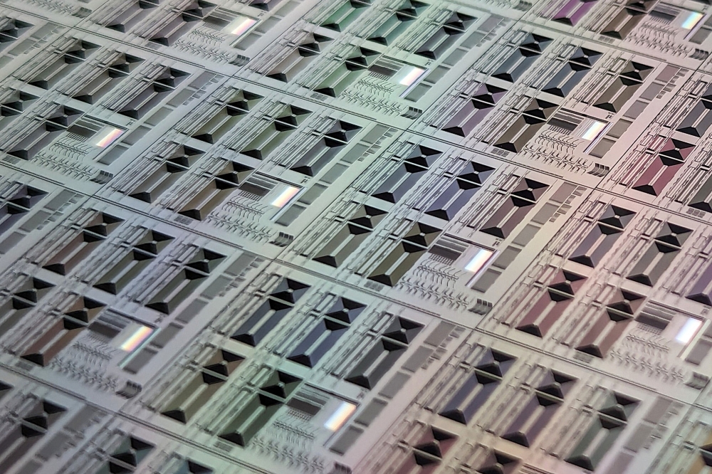
Aixtron delivers InP tool to Nokia
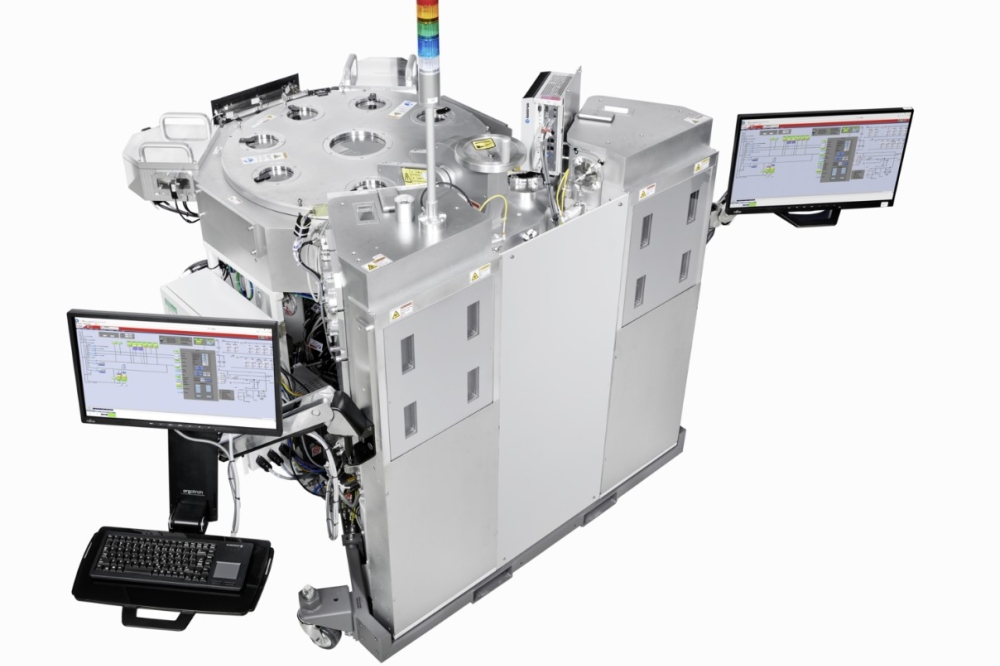
Aixtron SE will supply Nokia with its G10-AsP system to enable the company to produce 6-inch InP wafers, marking the next step in the evolution of photonic integrated circuits (PICs). This follows Nokia completion of its $2.3b acquisition of InP specialist Infinera, in late February 2025.
The G10-AsP system is designed to provide precise and uniform processes that PICs require in contrast to traditional transceivers, as demonstrated in particular on 6-inch InP wafers.
For example, thanks to an innovative injector and advanced temperature control the platform offers up to 4x superior on-wafer-uniformity for critical layers compared to the previous generation, according to Aixtron. Combined with In-Situ Cleaning, the company says these new levels of uniformities can be consistently reproduced without the need for hardware exchange or calibration between the different growth steps of the complex circuits. The automated Cassette-to-Cassette (C2C) wafer loading ensures highest operator efficacy for the MOCVD tool.
"We are thrilled to support Nokia’s innovation in photonic integrated circuits with our G10-AsP system. The ability to produce 6-inch InP wafers will significantly enhance their manufacturing and technology capabilities and drive the adoption of next-generation optical technologies," said Felix Grawert, CEO and president of Aixtron SE.
Steve Stockman, who leads Nokia’s InP-based PIC manufacturing added: "The acquisition of Aixtron's state of the art G10-AsP platform is a strategic investment in our production capabilities. This advanced technology will enable us to meet the growing demand for high- performance photonic integrated circuits and expand our leadership in the industry."


