Driving the next high-volume sensor revolution
Zero Point Motion is pioneering photonically enhanced inertial sensors, revealing how silicon photonics can break free from datacentres and become ubiquitous in everyday devices, but this transformation will require industry-wide cooperation.
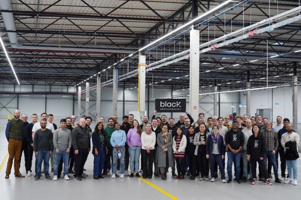
By Lia Li, CEO and founder, Zero Point Motion
There is no doubt that photonics is poised to transform the future, by enhancing existing technologies and enabling entirely new applications. My mission, and the reason I founded Zero Point Motion, is to answer one question: how do we bring photonics into everyday life?
Today, datacentres dominate high-volume photonics. They are massive, well funded, and rely on optical interconnects to power cloud computing and AI. This is “high volume but hidden away” – a market few consumers ever see directly.
Yet there’s another high-volume future awaiting silicon photonics – one where photonic components reach the hands of the public in everyday environments. Imagine optical technology in smartphones, automobiles, VR headsets, or even home appliances. If these use cases truly take off, photonics could become as ubiquitous as electronics, bridging the gap between specialised labs and the mass market.
From my vantage point, the hold-up isn’t a lack of ideas or even demand. Organisations are diving into photonic research for everything from quantum computing and telecoms to LiDAR and non-invasive biosensing. The real problem lies in scalability, standardisation, and packaging.
These hurdles were echoed at the Málaga Global Photonics Economic Forum in October 2024, where panellists discussing the question “Is photonics a semiconductor technology?” noted that a “lack of standardisation is due to companies not wanting to give up their IP,” and that “the photonics industry has an emotional attachment to very small performance gains, even when it makes the technology non-manufacturable” [1]. This highlights a cultural challenge within photonics: the drive for incremental improvements can overshadow the need to build reproducible, scalable solutions.

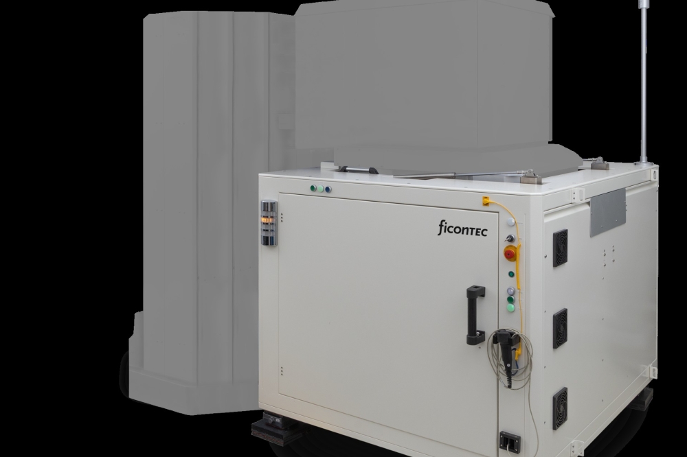
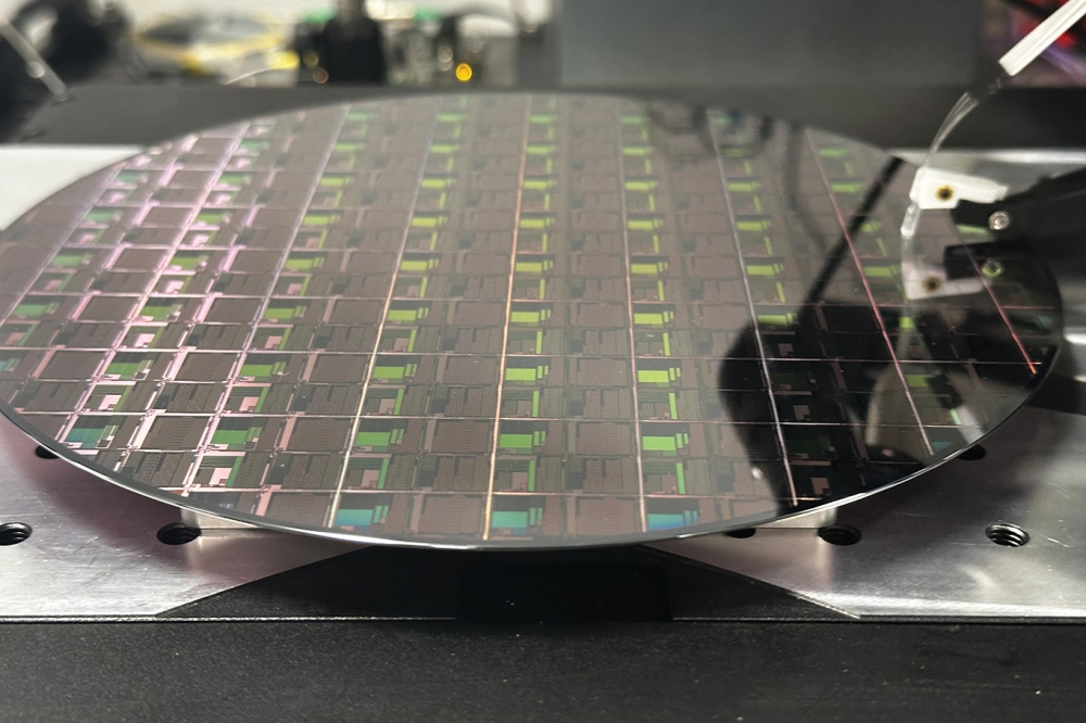
Lia next to the ZPM semi-automated wafer prober which combines
industry-grade equipment but with custom automation protocols and image
recognition.
Interestingly, there’s a parallel to draw with the world of micro-electro-mechanical systems (MEMS). Unlike silicon photonics – which at least has process design kits (PDKs) to guide design and fabrication – MEMS manufacturing is notoriously custom and lacks an equivalent degree of standardisation. Yet MEMS has grown into a multi-billion-dollar industry, with some reports estimating its global value at around $16 billion. How did it get there? By thriving in diverse, high-impact applications, from automotive airbags to smartphone accelerometers to microphones, and overcoming its customisation challenges with robust foundry support, co-integration with CMOS, economies of scale for mass adoption, and relentless demand for miniaturised sensors.
In many ways, MEMS succeeded because of its customisation, not despite it. Being able to tailor designs for specific automotive, industrial, and consumer needs has delivered high-value products that competing sensor technologies have struggled to match at volume. Over time, specialised design tools, improved packaging, and greater supply-chain maturity made large-scale manufacturing more predictable. The lesson for photonics is clear: if we can leverage existing foundry processes, invest in packaging research, and tap into strong market needs, then high-volume silicon photonics can follow a similar trajectory.
Inertial sensing as a beachhead
At Zero Point Motion, we use photonics to build precise inertial sensors that track movement by measuring how a small silicon structure inside the sensor shifts in response to applied motion – just as you feel yourself sway when a car speeds up or turns. Inertial sensing is an area where existing low-cost solutions often reach performance ceilings, meaning that photonics can deliver a decisive improvement in accuracy. By replacing capacitive readout with optical sensing, we aim to achieve higher sensitivity, lower drift, and better robustness – key factors for applications ranging from industrial automation to robotics and augmented reality.
Imagine a drone mapping a subterranean tunnel, a robot navigating a city’s high-rises to deliver goods, or a vehicle finding its way through an underground car park. These are all scenarios where signals from global navigation satellite systems (GNSS) drop out or become unreliable due to multipath errors, whereby signals are reflected off obstacles in the surroundings, taking longer to be received. A more stable inertial measurement system can step in to maintain accurate positioning when GNSS is temporarily weakened or unavailable. If photonic inertial sensors offer superior drift performance, we can push the boundaries of autonomy, especially when combined with advanced sensor fusion and AI navigation algorithms.
Crucially, to build the chips that underpin these sensors, we’re not demanding exotic foundry setups; we’re leveraging the same standard PIC processes already available in commercial fabs. Our goal is to show that photonic inertial sensors can be mass-produced on existing lines with minimal disruption to match the volumes of MEMS sensors shipped today.
Our sensors at ZPM harness the best of both worlds: MEMS for the large-mass mechanical response to a device’s motion, and silicon photonics for ultra-sensitive optical readout. This approach represents the next step in the evolution of inertial sensing – akin to how companies like InvenSense once took a bold wafer-scale risk, stacking different semiconductor processes atop each other to revolutionise MEMS fabrication and integration with application-specific integrated circuits (ASICs).
By integrating optical waveguides with MEMS structures, we can eliminate many limitations of traditional inertial measurement units (IMUs), drastically reducing signal noise and drift while unlocking new possibilities in sensor design and signal processing. Specifically, we leverage the evanescent field of photonic waveguides and ring resonators to couple properties of light – like resonance features – with the motion of MEMS structures. As the MEMS moves within that evanescent field, subtle shifts in position alter the effective refractive index around the waveguide, changing the resonant frequencies of the optical cavity. This enables ultra-precise motion detection without the drawbacks of electrical noise or external interference. There’s also a dissipative effect that broadens the resonance, increasing sensitivity and resolution even further.
A call for standardisation and industry cooperation
As exciting as photonic IMUs are, we face a harsh reality: without industry standardisation, start-ups can find themselves waiting months for a tape-out, then facing equally lengthy delays for packaging and integration. That’s a timeline many start-ups cannot survive in.
At Zero Point Motion, we’ve chosen to take on a lot of these processes in house. We perform our own automated wafer-scale probing, fibre-array attach, photodetector attach, laser-on-submount integration, and packaging – compressing the time from design to prototypes. By removing multiple handoffs and dependencies, we can iterate more quickly – up to two months faster – to refine our designs and reach working prototypes in a fraction of the time that a fragmented supply chain would impose.
Yet no single company can do this alone, and we certainly cannot get to production this way. We need industry-wide alignment on a few fronts. Many ecosystem players remain hesitant to share IP or adopt universal design kits and standards, slowing innovation and adoption. While foundry PDKs are an essential first step, a key takeaway from the 2024 PIC International Conference was that 80 percent of photonic value lies in packaging. To accelerate progress, the industry must advance proven equipment, standardised processes, and accessible entry points for new players. Establishing these will build confidence, reduce prototyping time, and speed up market entry.

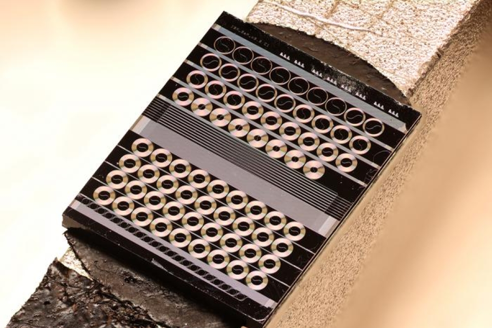
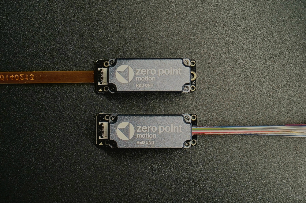
Early prototypes showing both fibre-pigtailed and fully integrated devices.
Photonics for AI gets plenty of headlines, but other promising applications, like sensing, can also drive the volumes necessary to make photonics mainstream. The industry as a whole stands to gain from championing multiple high-volume use cases, not just one. By building more predictable supply chains, smaller packaging solutions, and open standards, we can unlock an ecosystem that scales photonics as easily as we now scale MEMS or CMOS-based processes.
The sensor revolution is at a crossroads. Photonics can remain a niche technology, confined to specialised or high-end datacentre applications, or it can leap into everyday devices, treading the path MEMS sensors have taken over the past few decades. From my perspective, the choice is clear: we have to go big. By integrating photonic and MEMS platforms in ways that leverage existing foundries and packaging lines, we can unlock that next wave of scalable, high-performance sensors. From medical monitoring and automotive LiDAR to AR/VR motion sensing and robotics, there’s no shortage of markets eager for greater precision and reliability.
However, we won’t get there by inching forward with incremental improvements and proprietary processes. We need a unified push – from conferences to consortia – to standardise what we can, invest in robust packaging solutions, and open up to collaborative, cross-company efforts. If we do that, I believe that the next decade will see photonic sensors reach ubiquity, becoming woven seamlessly into consumer and industrial devices worldwide.