Lightwave Logic PDK for silicon photonics and EO polymer integration

The company says the PDK uses its novel BEOL process, enabling seamless integration of its EO polymers with silicon photonics while maintaining compatibility with existing semiconductor fabrication lines
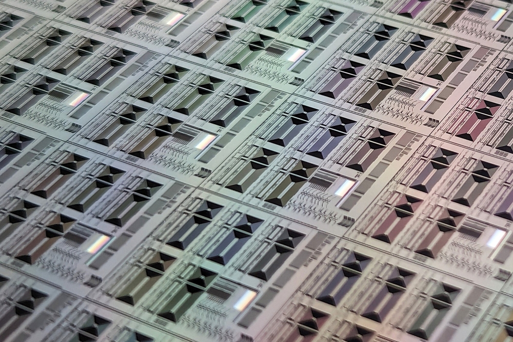
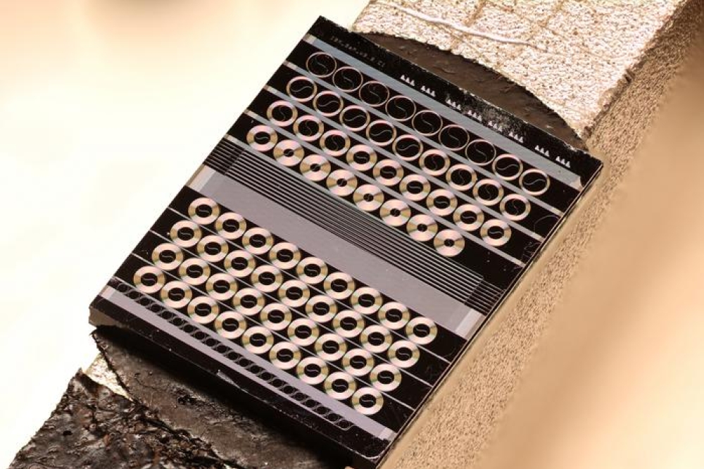
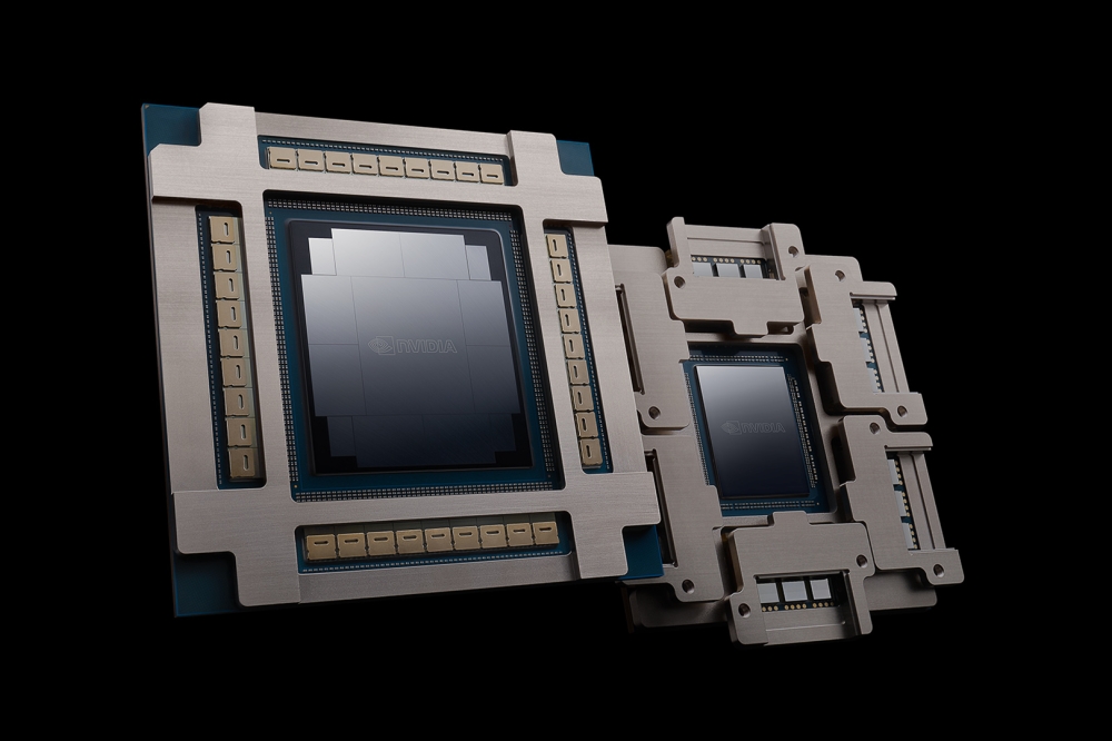
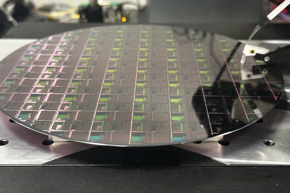
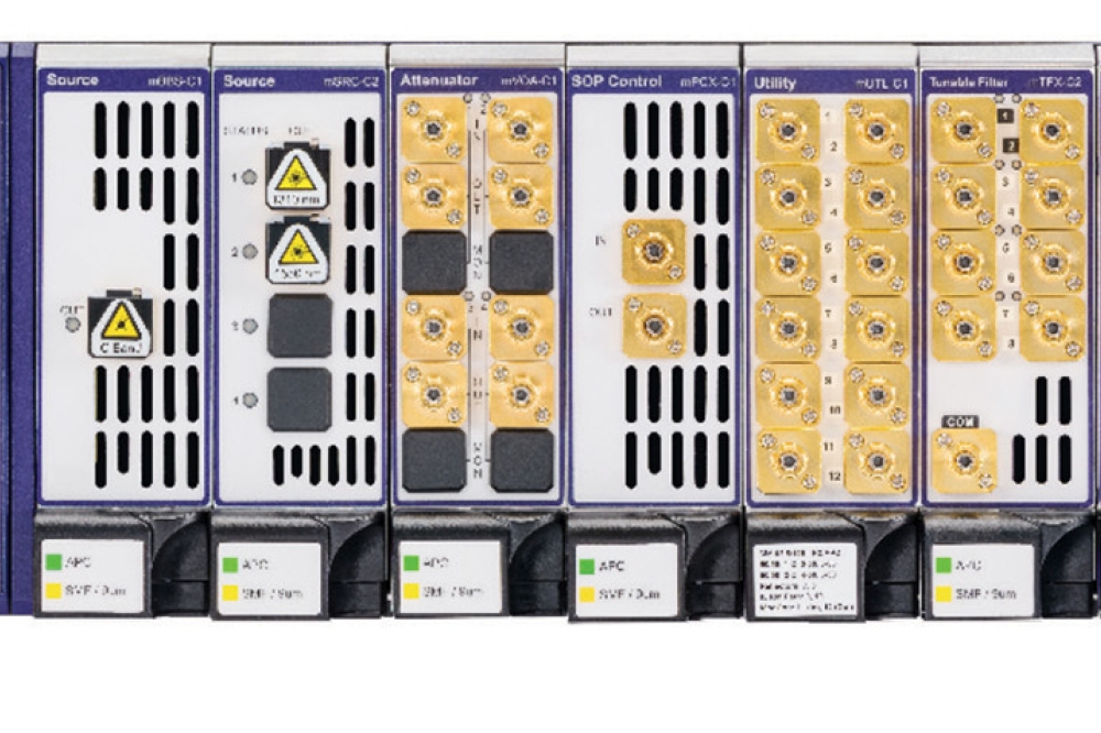
Lightwave Logic has announced the controlled availability of its Process Design Kit (PDK), which enables the integration of its advanced EO polymers into silicon PICs using its novel back-end-of-line (BEOL) process.
Despite the significant advancements in silicon photonics, scaling up to data rates of 200G and 400G presents inherent challenges. Traditional silicon photonics-based modulators face bandwidth limitations due to their reliance on charge-carrier effects, leading to increased power consumption and signal degradation at higher speeds. As datacentre and AI-driven networking demands continue to push for greater bandwidth efficiency, alternative materials such as EO polymers could play a disruptive role in overcoming these bottlenecks. According to Lightwave Logic, polymers offer ultra-fast response times, low power consumption, and high electro-optic coefficients, making them a compelling solution to enhance the performance of silicon photonics beyond its conventional limits.
Consistent with its mission to augment silicon photonics performance to meet the stringent bandwidth and power consumption needs of AI and networking applications across multiple generations, Lightwave Logic says its groundbreaking BEOL process encompasses key steps including EO polymer application, patterning and etching, atomic layer deposition encapsulation, EO polymer poling, contact pad opening, chip dicing, and end face creation and polishing. Crucially, the BEOL process is designed for compatibility with existing semiconductor fabrication lines, facilitating seamless integration with silicon photonic device manufacturing flows, the company adds. This process aims to offer flexibility, applicable at both wafer and chip levels up to the dicing stage.
Lightwave Logic says this advancement marks a significant step forward in the development of high-performance devices capable of 3.2T and beyond while preserving silicon photonics' unique cost and scalability advantages compared to alternatives such as thin-film lithium niobate or indium phosphide, which is crucial to the future of the industry.
“Our cuting-edge PDK represents a pivotal development in integrating our advanced EO polymers with silicon photonics,” said Yves LeMaitre, CEO of Lightwave Logic. “By offering a BEOL process compatible with existing semiconductor fabrication lines, we enable our partners to seamlessly enhance their silicon photonic devices, meeting the ever-increasing demands for higher bandwidth and lower power consumption in AI and networking applications.”
This PDK has already been implemented as part of collaborative efforts with two semiconductor foundries. Lightwave Logic says these demonstrations highlight the PDK's potential to accelerate the commercialisation of EO polymer-enabled silicon photonic devices, reinforcing the company's leadership in next-generation optical technologies.