A PIC laser designed for reliability and volume production
In the era of massive AI data compute and transmission demand, optical chip innovations must look beyond basic performance metrics with designs that accelerate PIC manufacturability.
By Yosef Ben Ezra, CTO, NewPhotonics
As AI applications continue to reshape our daily lives, we are witnessing a real-time pivot by hyperscalers and datacentres to meet the technology’s unique cluster compute and connectivity needs. Hyperscalers owned by giants like Google and Microsoft are building new configurations based on silicon photonics, which has been shown to improve energy efficiency and bandwidth benchmarks while reducing latency. Yet, while the technology advantages are known, these datacentres are now relying on the photonics and microelectronics ecosystem to demonstrate that silicon photonics manufacturing can be scaled to mass production.
While silicon photonics hold immense potential, one of the main challenges that remains is the integration of lasers.
There are various approaches to laser integration on silicon substrate that target improved laser coupling efficiencies, reliability, and testability. However, some techniques come at the cost of performance trade-offs, and few offer meaningful gains further along the design value chain.
In contrast to microelectronics’ marriage to silicon, optical functionalities are inherently dependent on a variety of materials, and this presents a substantial scalability roadblock for PICs. Additionally, since optical interconnects are now sustaining exponential traffic growth, microelectronics and photonics technologies are tightly intertwined. Under urgent market pressures to fulfil the rapidly rising demand for energy efficiency and speed at minimal cost, photonics must quickly adopt an integration approach that meets both technical and business expectations.
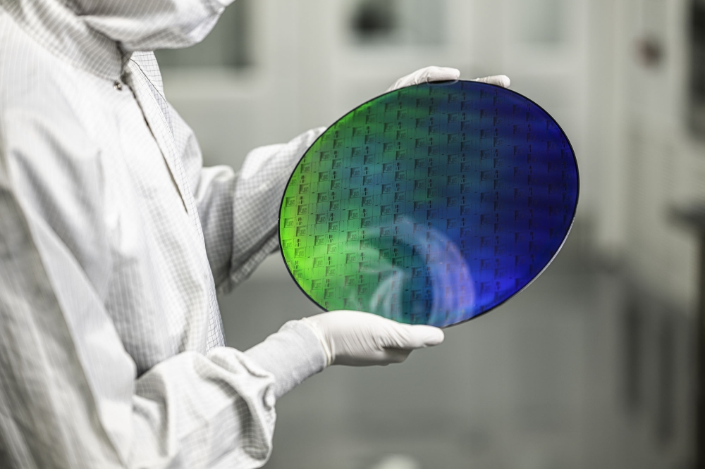
This year, NewPhotonics has answered that call with its NPG102 family of on-chip silicon PIC transmitter solutions. At the core of these products is a novel approach to heterogeneously integrating lasers at the wafer level. This development fast-tracks the paradigm shift in system design to enhance module yield maturity and reliability, boosting both efficiency and efficacy. By eliminating process steps in assembly and testing, this new technique reduces failure risks and enables output scaling, thus offering a solution to critical manufacturing and performance questions for transceiver module design.
Demonstrating greater than 90 percent efficiency (< 0.5 dB loss) in laser coupling alone, this innovation supports OEMs and system integrators to overcome current barriers and deliver what datacentres and hyperscalers are eager to implement. This article will examine the challenges associated with laser integration and packaging options, focusing on external coupling and discrete components, while also exploring how a shift towards scalable technologies can accelerate the adoption of silicon PIC solutions in datacentres. A comparison of various laser integration technologies is provided in Table 1.
Transitioning to heterogeneous integration
A growing number of methods for integrating PICs with lasers in transceiver module designs focus on gradually improving attachments to external components. However, while sourcing, aligning, testing, and managing lasers in new ways may achieve incremental gains, few options deliver significant leaps in performance and reliability, or offer greater manufacturability.
The challenge of coupling the laser energy output into a waveguide is ultimately solved by designing an optical mode-matching solution that promotes low-loss power transfer between the two elements. Precise physical alignment between the laser output and the waveguide is necessary but not sufficient; without careful three-dimensional design to accommodate the optical mode, the power transfer will not be optimised and coupling losses will increase. Attempting to couple discrete components is therefore limited by the lack of customised mode-matching design, meaning that more intimate integration between the laser and waveguide is a necessity for energy-efficient silicon PIC solutions in the datacentre and for scalable manufacturing.
Applying a more tightly aligned integration approach using wafer bonding to integrate III-V materials such as indium phosphide (InP) onto silicon substrates enables laser fabrication directly on silicon photonic platforms. This integration improves precision, density, and manufacturing efficiency. The transition between III-V laser structures and silicon waveguides is achieved through optimised bonding techniques and the design of rib or ridge waveguides to confine light effectively.
Direct wafer bonding generally involves three steps: surface treatment, room temperature bonding, and thermal treatment for bonding energy enhancement. The smooth, clean surfaces ensure efficient optical coupling and minimise losses. Some techniques involve deposition of self-assembled monolayers (SAMs) of an organic material and provide flexibility so that the surface chemistry can be adjusted to accommodate a variety of materials. Wafer bonding is crucial for creating silicon-on-insulator (SOI) substrates and enabling compact photonic devices, such as integrated waveguides and coupling mechanisms.
Manufacturers can create high-quality InP layers on silicon through methods like Epitaxial Lateral Overgrowth (ELOG) and Selective Area Growth (SAG). These InP layers serve as active gain mediums for the different kinds of lasers that can be formed, such as Fabry-Perot, Distributed-feedback (DFB), Distributed Bragg reflector (DBR) and ring resonator lasers. To achieve good coupling between the laser and waveguide on the chip, fabrication techniques must overcome challenges including lattice mismatch, thermal expansion differences, and defects such as stacking faults.
The silicon confinement factor – a measure of how much light remains trapped inside the silicon core of a photonic device, such as a waveguide – is an important parameter in determining coupling efficiency when a laser device is integrated with silicon passive devices. In silicon photonics, high confinement is typically desired because it allows the device to efficiently guide light within the silicon core, improving performance and minimising signal loss. The silicon confinement factor depends on the geometry of the waveguide and the refractive index contrast between silicon and the surrounding materials. Typically, the III-V mesa – a structure designed to guide the laser light – is wider than the silicon waveguide. This means that the confinement of the transverse mode is determined by the SOI waveguide and not the III-V mesa. This eliminates any issues with alignment of the III-V etch to the SOI etch. Figure 1 shows an optimised mode matching for efficient coupling between the III-V laser and silicon waveguide.

Figure 1. Optimised mode matching for efficient coupling
between III-V laser and silicon waveguide.
Eliminating failure points with laser on silicon
The drive to ‘illuminate silicon’ and close the gap between the photonics and microelectronics industries is no longer merely an attractive prospect—it is now an essential goal. However, to turn this vision into a commercially viable reality, the industry must overcome silicon’s inherent material limitations: its indirect bandgap and the lack of a linear electro-optic (Pockels) effect, both of which make it challenging for silicon to emit or manipulate light. Leveraging mature CMOS infrastructure, the NewPhotonics design addresses this challenge by creating a ‘shortcut’ for photonics and eliminating the deficiency in integration technology.
Compared with the tricky alignment of a laser diode to a silicon photonic chip in the final stage of packaging, the integration of III-V on silicon represents a major technological breakthrough. Central to the NPG102 design are thin films of InP integrated through wafer bonding in a process similar to epitaxial growth of optical gain materials on large-scale silicon wafers. This platform also enables multiple technical merits favourable to laser design, operation, and integration of active and passive components.
From a fabrication perspective, this integration shifts laser functionality from being the last manual chip-level production stage to an earlier and automatic CMOS-like manufacturing stage. Since the active alignment and accuracy requirements for external lasers place a substantial burden on manufacturability and scaling, the move to integrated lasers represents a profound improvement in terms of fabrication precision, integration density, production volume, and efficiency. By reducing the need for added components, we also eliminate the points of failure caused by issues in coupling that could otherwise impact signal quality.
The financial advantages of integrating lasers are also clear. Discrete components demand added equipment and assembly steps when laser integration is external to the PIC. Eliminating engineering resources and instruments for laser-lens attachment, wire-bonding, and auto-alignment significantly reduces costs and speeds up production schedules, accelerating yield maturity rates and time to market, often by several months.
Significant logistics overhead may also be reduced without the need for separate device procurement, reliability, and vendor management. Historically the slow and labour-intensive packaging of discrete components in optical transceiver products has traditionally resulted in low-volume and expensive technology, with packaging typically contributing up to 80 percent of the total cost. Approximately half of this packaging expense is due to external laser integration, demonstrating an opportunity for considerable cost savings with integrated lasers.
On the performance side, this integrated design vitally enhances the coveted property of laser reliability to the extent that integrated lasers have become the technology of preference for leading hyperscalers. The most common fault in transceivers is laser failure, but photonic devices with integrated lasers are less susceptible to environmentally triggered failures due to the encapsulation of the silicon-based process, as well as having fewer discrete parts. There are also no etched and coated facets that risk catastrophic optical mirror damage.This means that employing CMOS-like technologies for InP laser integration is the key to advancing dependable and consistent photonic integration and performance, impacting reliability and yield at the level of both the device and transceiver module.
In the ramping stage of a new transceiver integration line, using “Known Good Die” has huge advantages in shortening the time to yield maturity. Equally advantageous is the lack of laser coupling and integration and the associated learning curve in the production line. Moreover, we have witnessed impressive zero failure rate metrics in NPG102 chips over an extended test period, accentuating the enhancements in reliability and longevity that extend both the life of the laser and the opportunity to scale.

Table 1. A comparison of various laser integration techniques, their advantages, challenges, and coupling efficiencies.
Mode matching for integrated coupling
When external lasers are used in transceivers, the optical coupling loss reaches approximately 2.5 dB, due largely to the mismatch between the non-optimal, asymmetric mode of a DFB laser and the symmetric edge coupler input mode. Challenges with mechanical alignment require micron-level accuracy achieved through time-consuming active alignment techniques. Furthermore, reflections at the chip interfaces limit spectral flatness.
Integrated laser-to-waveguide coupling is a key element in heterogeneous photonic systems. There are several techniques for efficient coupling, including adiabatic, evanescent, and tapered coupling, among others. Table 1 summarises these methods and their advantages and disadvantages. Adiabatic coupling entails gradual transformation of the optical mode between the III-V laser and the silicon waveguide over a longer coupling region. Both materials have tapered waveguides that gradually merge, allowing efficient energy transfer. This offers low insertion loss due to the adiabatic nature of the transition, as well as better mode matching and higher bandwidth compared to abrupt coupling schemes.
In evanescent coupling systems, the laser output couples to the silicon waveguide through an overlapping evanescent field. The III-V gain region is bonded onto a silicon photonics platform, and a shared evanescent field region enables gradual energy transfer between the laser and the waveguide. This technique has higher fabrication tolerance, and better integration density and scalability, but it requires highly precise engineering of the bonding interface for refractive index matching. A silicon-on-insulator (SOI) platform is often used to enhance the optical confinement.
Tapered coupling, meanwhile, allows the gradual transfer of the optical mode from a III-V laser into a silicon waveguide. The III-V laser facet is tapered down, matching the size of the silicon waveguide mode, and mode size transformation minimises coupling losses. This approach is widely used in high-speed optical transceivers to ensure efficient coupling. However, precise, high-quality tapering requires advanced lithography and etching processes, increasing fabrication complexity.
The NewPhotonics approach overcomes the limitations and compromises of external coupling and instead establishes an environment where internal coupling options may be optimised or customised for better overall chip performance. By adopting advanced wafer-bonding techniques with a laser-integrated design, we diminish the complexities that negatively impact efficiency, reliability, and density, reducing both time and cost to transceiver delivery.
This novel approach to wafer-level heterogenous integrated lasers for silicon PIC-based interconnect modules represents a transformative shift in optical transceiver technology. The heterogenous laser integration achieves outstanding coupling efficiency that optimises laser efficacy with higher reliability in terms of both performance and manufacturability.
With the NPG102 we have jumped beyond the incremental attempts to integrate lasers with discrete component designs to address critical market and sustainability concerns. This process leapfrogs traditional external laser coupling methods, reducing optical losses, and improving overall reliability. Furthermore, this advancement simplifies datacentre infrastructure — accelerating the pivot to rack designs that use optics-driven interconnects with optimised power efficiency and signal quality.
This novel strategy for integrated lasers offers increased production yield metrics, improved reliability, and shortened time to market. In the highly competitive datacom transceiver market these differentiators combine for clear cost and efficiency advantages. The shift to heterogenous laser integration in silicon will bridge the module supply gap for high-capacity, low-latency, and power-efficient data networks, helping datacentres to meet the growing demands placed on network and compute volume by AI. This evolution is set to redefine datacentre performance and efficiency, making it an indispensable technology for the future of digital communications.