200G+ per lane: powering the next-gen data deluge

Integrated photonics is pushing the boundaries of data transmission, enabling speeds of 200G per lane and beyond. This leap forward promises to revolutionise datacentres and telecommunications, addressing the ever-growing demand for bandwidth driven by the proliferation of AI/ML.
By Adam Carter, CEO, OpenLight
Global data traffic is growing exponentially, with a huge increase in the amount of information created, consumed, and stored worldwide driven by trends like video streaming, the internet of things (IoT), and most significantly the rise of artificial intelligence and machine learning (AI/ML). As AI models grow in complexity and capability, the need for robust datacentre infrastructure is becoming more pressing than ever before.
Industry projections from JLL estimate that global datacentre storage capacity will soar from 10.1 zettabytes (ZB) in 2023 to a staggering 21.0 ZB by 2027, reflecting an annual growth rate of 18.5 percent. This demand requires network infrastructure capable of handling vastly higher data rates, pushing the boundaries of incumbent technologies. Current optical and electrical systems are struggling to keep pace, facing limitations in power efficiency, thermal management, and scalability.
A target in this evolution is PICs that can achieve 200G per lane, a milestone representing a significant leap forward in data transmission speeds. But scaling to 200G and beyond presents numerous challenges, including thermal management, power efficiency, signal integrity, and manufacturing scalability. Moreover, these hurdles are compounded by the increasing complexity of chip designs, the need for new materials and interconnect technologies, and the ever-present pressure to reduce costs. Utilising a heterogeneous PIC offers a 50 percent cost saving by leveraging the economies of scale of a commercial silicon foundry process versus the conventional manufacturing process for a transmitter optical sub-assembly.
While photonic technologies typically generate less heat per bit than electronic ICs, rising data rates mean that PICs, too, must incorporate effective thermal management strategies to ensure reliability and performance. Some high-speed solutions require thermoelectric coolers (TECs), but these have the drawback of increased power consumption. OpenLight’s solutions, meanwhile, can avoid TECs altogether, thus offering better power efficiency.
Photonics also offers inherent energy advantages over traditional electronics, but maintaining low power consumption at ultra-high speeds remains a hurdle due to the energy needed to operate active components such as lasers and modulators, which are necessary for manipulating light signals effectively. This technology achieves over 40 percent power savings compared to traditional methods. By leveraging heterogeneous integration for superior waveguide coupling, this method significantly reduces the drive voltage needed for the desired output power. Furthermore, InP modulators require lower drive voltages than silicon modulators at 200G per channel, further contributing to energy efficiency.
When it comes to signal integrity, preserving quality over long distances and at such high speeds requires innovative design approaches, including advanced modulation formats and robust error-correction mechanisms. Traditional PICs, relying on external components, also face limitations in size, cost, and manufacturability, making them unsuitable for widespread deployment at higher speeds.

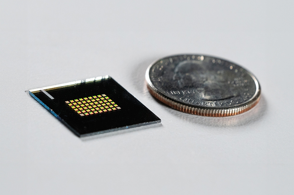
The OpenLight 1.6T DR8 PIC
To meet the demands of next-generation datacentres and AI infrastructure, OpenLight is developing the 1.6T DR8 PIC, which supports 200G-per-lane architectures. Currently at the alpha sampling stage, it represents remarkable progress in heterogeneously integrated silicon photonics and incorporates several features designed to address the critical challenges of high-speed data transmission.
To achieve high-performance 1.6T DR8 PICs, two key technologies are essential: distributed feedback lasers (DFBs) and electro-absorption modulators (EAMs). DFBs are used for their ability to provide a stable and precise light source, crucial for high-quality signal generation. EAMs, meanwhile, are used to modulate the light signal, encoding data onto it at incredibly high speeds.
OpenLight’s 1.6T design includes both of these core enabling elements. Power-efficient DFBs serve as the PIC’s light source, with integrated semiconductor optical amplifiers mitigating optical losses at 200G. This not only enables unprecedented data rates but also lays the foundation for future 3.2T infrastructure running at 400G per lane, a critical requirement for the continued growth of AI networks.
The EAM technology that OpenLight employs is particularly noteworthy, offering high-speed operation proven to over 65 GHz and targeting 100 GHz+ for 400G-per-lane support. At the same time, the PIC is small in size to allow for tight integration, temperature independent to eliminate the need for external cooling, and can be driven with differential or single-ended drives at low voltage. The 1.6T DR8 PIC achieves all this in a compact 37 mm² form factor and consumes a maximum of just 2.2 W, demonstrating exceptional energy efficiency.
The OpenLight platform: empowering innovation
Beyond developing our own technology, we are also acting on our commitment to an open platform and this is changing the game for the photonics industry. By providing Process Design Kits (PDKs) to foster a collaborative ecosystem, we are empowering companies to develop their own custom PIC solutions. Partnering with key players like Tower Semiconductor, Synopsys, and others will further strengthen this ecosystem to provide designers with the tools they need to succeed.
The future of data transmission hinges on the ability to move information at ever-increasing speeds. Breaking the 200G barrier represents a leap towards that future. As data demands continue to grow rapidly, innovations like heterogeneously integrated silicon photonics with DFBs and high-speed EAMs will be essential to driving progress.
The continuous evolution of the PIC market fuelled by advancements in integrated photonics will open new opportunities in applications like 5G/6G networks, quantum computing, autonomous systems, and medical diagnostics. At the same time, industry-wide adoption of heterogeneously integrated PICs will drive standardisation and reduce fragmentation in the photonics ecosystem, creating a more streamlined approach to designing and manufacturing photonic systems.
OpenLight’s technology promises to reshape datacentres, power the next generation of AI, and impact a wide range of fields, while our open platform is helping to cultivate a thriving industry that will be ready to meet the data needs of tomorrow.