Revolutionising telecoms with the world’s smallest fully optical amplifier

A compact erbium-doped waveguide amplifier achieves record-breaking performance, heralding a new era for integrated photonics in data communication, sensing, and beyond.
By Parsa Khorasani, Photonics Engineer, EDWATEC
In today’s digital age, where information flows faster and
in higher volumes than ever before, optical amplification has become essential
to global communication infrastructure. Whether streaming high-definition
content or transferring terabytes of data within or between datacentres or
across continents, activities of modern telecommunication networks would not be
possible without the ability to amplify light signals with minimal noise.
Central to this capability are erbium-doped fibre amplifiers (EDFAs). Since their invention in the 1980s, EDFAs have revolutionised the telecoms industry by effectively boosting signals travelling through optical fibres, enabling seamless, long-distance data transmission across vast networks, including across the Atlantic Ocean.
Erbium’s remarkable success lies in its unique ability to amplify light in the 1.55 µm wavelength range, which coincides with the region of lowest transmission loss in silica fibres, making it the ideal choice for optical communications.
Erbium ions have a distinctive electron configuration and exhibit long-lived excited states when embedded in host materials such as glass or silica.
This property allows them to act as highly efficient gain media, simultaneously amplifying multiple optical channels with exceptional stability, low noise figure, and without crosstalk. Over the decades, EDFAs have expanded their reach far beyond telecoms, finding critical applications in lasers, precision sensing, and even atomic clocks.

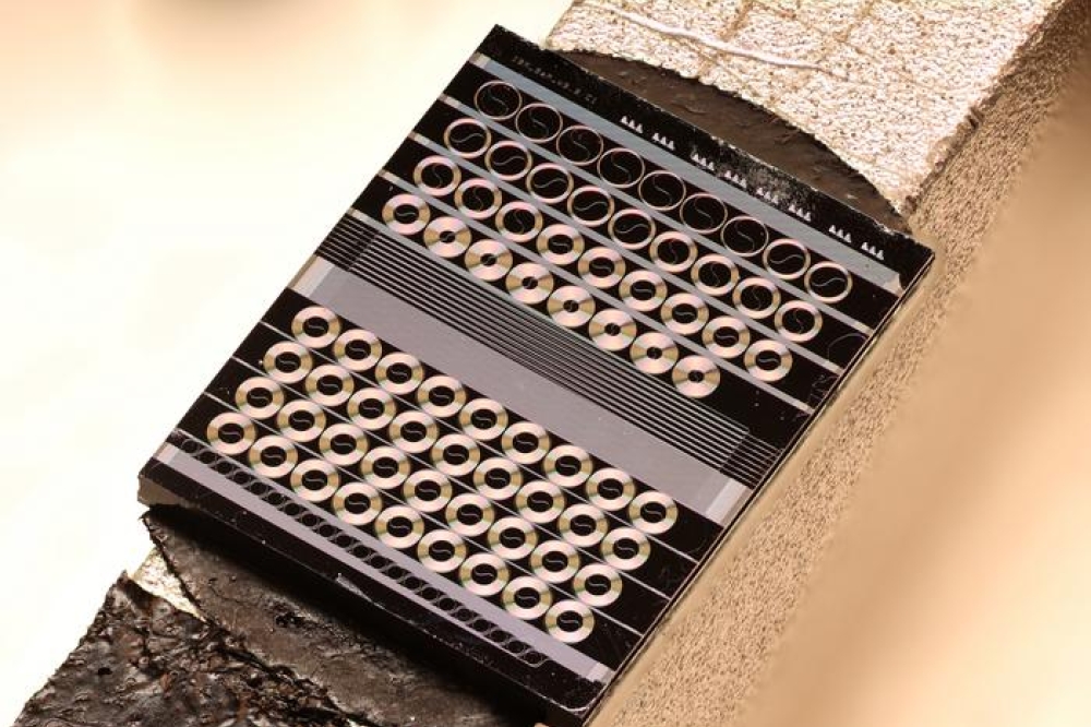
Figure 1. A 1 cm × 1 cm chip hosts multiple erbium-doped
waveguide amplifiers (EDWAs), each featuring a spiral waveguide design tailored
to specific performance characteristics. The visible green emission highlights
the optically excited erbium ions, showcasing the active amplifier within the
chip.
However, as the demand for data grows exponentially, driven
by AI, cloud computing, video streaming, and the proliferation of IoT devices,
traditional EDFAs are reaching their limits. This is particularly evident in
datacentre interconnects, where data rates have surged beyond 400G,
necessitating new solutions that align with the miniaturisation and integration
requirements of modern photonic systems. While EDFAs continue to be reliable
workhorses, their high cost, bulky fibre-based architecture, and large form
factor are increasingly at odds with the demands for compactness and
integration into next-generation photonic technologies. The need for efficient,
scalable, small-form-factor amplification solutions has never been more urgent.
But replicating the success of EDFAs in a compact, chip-scale format has been a longstanding challenge. As early as the 1990s, institutions like Bell Labs embarked on efforts to develop erbium-doped waveguide amplifiers (EDWAs), aiming to capture the same amplification properties of erbium within a scalable, integrated waveguide structure that could be incorporated into photonic chips.
However, these and other early attempts were met with significant obstacles such as high waveguide losses, stemming from imperfections in the fabrication processes. These losses severely limited the length of useable waveguides, thereby restricting the amplification potential and significantly reducing the achievable gain. Additionally, the phenomenon of cooperative upconversion or pair-induced quenching—where energy is lost due to interactions between densely packed erbium ions—further reduced efficiency and limited the achievable gain.
Despite significant advancements in photonic integration technologies, all attempts to create integrated erbium-doped amplifiers had, until recently, struggled to exceed output power levels beyond a milliwatt, falling well short of the performance achieved by their fibre-based counterparts.

Figure 2. Experimental setup of a multi-lane erbium-doped
waveguide amplifier (EDWA) featuring an on-chip signal and pump mixing unit
(WDM) and an edge-coupled pump laser. This design enables massive
parallelisation of data transmission, a feat unattainable with traditional
EDFAs due to their large footprint or conventional OSAs due to high channel
crosstalk.
Founding EDWATEC on a technological breakthrough
Decades after the first attempts to develop EDWAs, a
groundbreaking advancement at the Laboratory of Photonics and Quantum
Measurements (LPQM), led by Tobias Kippenberg, a professor at EPFL, has led to
a dramatic shift in the field. By integrating ultra-low-loss silicon nitride
waveguides with precise ion implantation techniques, the LPQM team achieved an
erbium-doped waveguide amplifier with an extraordinary output power of 200 mW.
With a small-signal gain exceeding 30 dB, this results in more than 1000-fold signal amplification—all on a chip measuring below 5 mm2 in footprint, making it the world’s smallest fully optical amplifier. This EDWA provides stable gain with a low noise figure, while remaining resilient to crosstalk, non-linearities, and temperature fluctuations.
The innovation lies in the meticulous engineering of the silicon nitride waveguides and the ion implantation. By reducing background losses, the researchers have demonstrated designs featuring up to 50 cm of waveguide length in a compact spiral configuration, maximising the interaction length between light and the erbium-doped material. This novel integration strategy allowed the team to overcome decades-old barriers, setting a new benchmark for chip-scale optical amplifiers, and paving the way for the founding of EDWATEC, a company that is now commercialising this cutting-edge technology.
One of the primary industries set to benefit from EDWAs’ versatility is the growing market for coherent transceivers, especially for datacentre interconnects (DCIs). As data traffic between hyperscale datacentres surges, driven by AI workloads and massive data analytics, the demand for high-capacity, low-latency optical links has intensified. DCIs, typically spanning distances of 10-120 km, now require transmission rates that have skyrocketed from tens to hundreds of gigabytes and beyond in the span of just a few years. With the emergence of new terabyte communication systems, the critical role of advanced optical amplifiers becomes even more pronounced.
Traditional amplification technologies, such as EDFAs, face considerable challenges in this evolving landscape. Their fibre-based design limits scalability and integration within modern photonic platforms, while their high production costs present significant barriers to widespread adoption. EDWAs offer a transformative alternative; their compact form factor, compatibility with silicon photonics, and wafer-scale manufacturability enable the integration of multi-lane amplification on a single die. This breakthrough addresses a critical bottleneck in high-bandwidth, dense network environments, offering unprecedented scalability and efficiency for coherent transceivers and unlocking new capabilities for DCIs.

Figure 3. Fully hybrid in-house packaged integrated external
cavity erbium laser, featuring an edge-coupled pump diode and broad wavelength
tuneability.
Deep-sea cables to satellite networks
DCIs are not the only application that EDWAs have the
potential to transform in the coming years. Their compact size, high power
output, and ability to operate efficiently in extreme environments position
them as a key enabler of next-generation technologies across several critical
domains, including communication, sensing, and mapping.
From deep-sea fibre optic networks to satellites orbiting Earth, EDWAs represent a versatile and scalable solution to the diverse amplification challenges faced in modern photonics.
In undersea optical communication networks, where amplification units are typically spaced every 80 km within tightly constrained repeater stations, EDWAs’ minimal footprint provides a significant advantage. Traditional EDFAs face physical scaling limitations as the number of fibres in a single cable increases.
In contrast, EDWAs offer high-power amplification in a fraction of the space, enabling the integration of multi-channel amplification within a single module.
EDWAs are also well suited for optical links in free-space satellite communications; their compact size and lightweight design make them ideal for systems where minimising payload weight and maximising available space are essential to reduce launch costs and optimise functionality. EDWAs’ small footprint enables higher integration densities, allowing multiple amplifiers to be incorporated into limited satellite space. Additionally, silicon nitride-based EDWAs demonstrate exceptional resistance to radiation and environmental stresses, ensuring reliable operation in the harsh conditions of outer space.
LiDAR (light detection and ranging) systems are yet another area that stand to benefit from EDWAs. These systems are critical for applications ranging from autonomous vehicles and precision mapping to meteorological surveillance and forecasting. Once more, the high gain and compact designof EDWAs enable them to amplify low-power laser signals to the required levels for long-range sensing. Besides the direct advantages of EDWAs, their development has also driven more general advancements in erbium-doped PICs. An exciting by-product of this research is the invention of a new type of laser: integrated external cavity erbium lasers. These devices are distinguished by their ultra-narrow linewidth, which reaches as low as 50 Hz, ensuring the high spectral purity that is critical for precision applications in optical communication, sensing, and beyond. Additionally, they demonstrate remarkable stability, with temperature insensitivity enabling consistent performance across a wide range of environmental conditions.
Another standout feature of these lasers is their ability to lase across the C-band and L-band – spectral regions that are vital for modern optical networks. EDWATEC achieves this broad tuneability using thermo-optic effects, enabling precise wavelength selection and allowing these devices to support a diverse array of applications.
With their compact form factor and ability to achieve low noise, high output power, and wide wavelength tuneability, integrated external cavity erbium lasers bridge the gap between traditional fibre-based systems and state-of-the-art semiconductor lasers. Their reliability and exceptional performance characteristics make them an indispensable tool for applications, notably in fibre sensing, spectroscopy, LiDAR, and communications.
Silicon photonics integration and scaling EDWAs
The next phase in EDWA development focuses on seamlessly
integrating them into silicon photonics platforms to meet the demands of
diverse communication systems. EDWATEC is exploring two primary approaches:
heterogeneous integration, which incorporates EDWAs into existing platforms via
hybrid techniques, and monolithic integration, which takes advantage of the
amplifiers’ compatibility with silicon photonics to embed them directly onto
the photonic chip, ensuring a streamlined and homogeneous process flow.
Successful integration requires precise alignment with the specific fabrication workflows and application requirements of each customer.
EDWATEC therefore tailors its integration strategies to ensure optimal performance in diverse real-world scenarios, including high-speed datacentres, telecommunication networks, and undersea communication systems.
The company also provides custom-designed EDWAs, meticulously optimised to meet the unique specifications of each application. This involves addressing the nuanced challenges posed by various deployment environments, ensuring that each solution delivers reliable and high-performance amplification. Looking ahead, EDWATEC aims to accelerate the commercialisation of EDWA technology through collaboration and supply agreements. This will enable clients to fabricate and integrate amplifiers within their own facilities, reducing production costs and lead times while granting full control over the integration process. This strategy marks a significant milestone in establishing EDWAs as a scalable, industry-standard solution for next-generation photonics. To enable large-scale production of EDWAs, the fabrication process is transferred to silicon photonics foundries, ensuring consistent quality and uniformity across high-volume manufacturing. EDWATEC collaborates closely with foundries to refine and optimise processes, adhering to stringent quality standards.
Additionally, applications such as deep-sea fibre optic links present unique challenges, requiring robust packaging solutions to withstand extreme conditions like high pressure, moisture, and mechanical stress. Scaling these packaging solutions for mass production is vital for deploying EDWAs in critical global infrastructure projects. EDWATEC is addressing these technical and logistical challenges, with the aim of establishing EDWAs as a scalable and reliable solution for demanding applications worldwide.
By enabling seamless integration within silicon photonics platforms where other functional components are already on-chip, EDWAs eliminate the need for bulky and costly fibre-based amplification, unlocking new possibilities for compact, high-performance transceivers that are not only more cost-effective, but also better suited for next-generation integrated solutions. From high-bandwidth datacentres to undersea communication cables and satellite communication systems, EDWATEC is dedicated to advancing the production, integration, and deployment of EDWAs to meet the ever-growing demand for faster, more energy-efficient, and reliable optical networks.