Driving functional test closer to the chip
As photonic chip designs become increasingly complex, test processes must co-evolve with the technology, helping to ensure PIC performance and reliability, reduce development costs, and drive widespread adoption of silicon photonics.
By R. Matthew Adams, Senior Product Manager, Photonic and Fibre Optic Test Solutions, Lab & Manufacturing Applications, VIAVI Solutions
Silicon photonics is a core technology enabling next-generation communication ecosystems. Recent advances in the area have been critical to delivering the 800G and 1.6T modules that underpin today’s AI infrastructure, datacentres, and coherent transport. Yet as process technologies mature, expectations grow, leading to a plethora of new technical challenges.
For instance, the increasing functional integration and the hybrid integration of new materials as a path to reduced power consumption both require improvements to process and device yields, which in turn enable the number and types of devices per chip. Hurdles also remain with cost-effective “fibre-attach” processes for high-fibre-count applications, such as co-packaged optics (CPO) devices.

Table 1. Optical tests occur at different stages along the
transformation chain, traditionally grouped into three key phases: wafer
level, packaged device level, and integrated modules like the OSFP or
QSFP. Each phase has unique requirements for both optical test function
and test system architecture.
Meanwhile, rising baud rates and symbol rates will require tighter performance tolerances. In many cases the need to “trim” or calibrate chip-level characteristics will become increasingly important to improve yield and performance. Additionally, data management processes for integrating values into the digital signal processors (DSPs) controlling the target modules will need to become more and more efficient.
In the face of this dynamic ecosystem with its various obstacles, optical testing will also need to change and evolve, capitalising on the opportunity to bring application-level testing or functional test closer to the chip as functional integration increases and fabrication processes mature. To understand how the industry can achieve this, we first need to look at the different kinds of tests routinely performed throughout product development, and what their purposes are.
Test engineers often divide test types into two categories: parametric and functional. For silicon photonics, a parametric test refers to a set of measurements taken on a photonic device to characterise its key optical properties. These include insertion loss, polarisation-dependent loss, bandwidth, and responsivity, with tests typically performed at the wafer level during the manufacturing process to identify potential issues early on.
A functional test, on the other hand, refers to a set of measurements conducted on a fabricated PIC to verify that it operates as intended, assessing its overall performance by evaluating parameters driven by the final application. This kind of evaluation determines whether the device meets its design specifications and will function properly within a system.

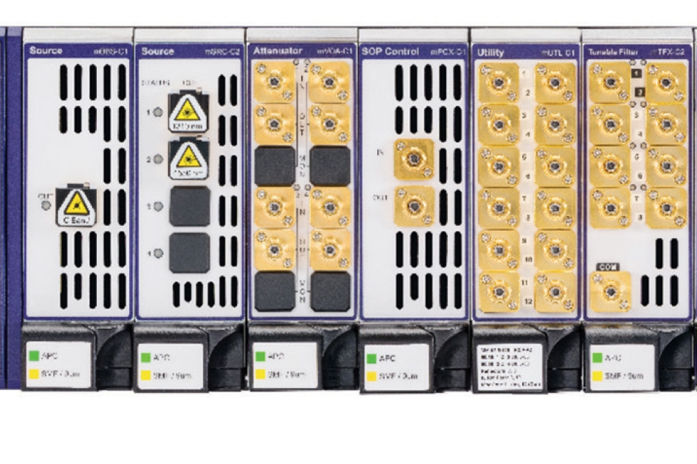
Figure 1. Modular platforms can be flexibly configured to deliver test coverage tailored to the needs of different optical functionality.
These tests can also be distinguished by purpose; parametric tests focus on the physical properties of a device, and are predominantly indicative of device geometry and material quality. They can be important in the early stages of a chip’s development and for tracking processing variation and, in many cases, they help take the chip from the lab to early manufacturing. However, as designs and processes mature, engineers may consider removing or reducing test coverage in these areas.
By comparison, device-level functional tests treat the chip as a system, measuring higher-level values. Testing here is much more focused and tends to occur at the intended operational wavelength and at a specified data rate, with tests such as bit error rate (BER) and transmitter dispersion eye closure quaternary (TDECQ) being used.
These tests are closely connected to final user specifications and include a range of transmitter powers (overload test). Results may look at the combined data from multiple structures and can be used to calibrate chip performance characteristics, such as optical losses impacting photodiode quantum efficiency, or the performance of polarisation beam splitting functions in coherent receivers.

Figure 2. Enabling triggering and real-time data streaming from the power meters in the VOA can dramatically simplify the provision of alignment feedback. When this action is complete, the VOA can be deployed for receiver sensitivity testing.
Testing along the integration path
Optical tests occur at all phases of the transformation chain. A traditional segmentation would be to group them in the following three phases: wafer, package, and module, as summarised in Table 1. Each phase has unique requirements for both optical test function and test system architecture.
Traditionally, lower-level tests of basic optical performance have had to be undertaken at the chip level, with higher-level tests deployed as technologies are integrated.
As chip complexity grows and processes mature, moving these functional tests closer to the silicon offers significant advantages, including a reduction in the number of test steps from the wafer through to the module. It also allows the yielding of chips before costly integration steps, and the simplification of final module tests through the reduction of testing overlap.
Migrating tests to earlier manufacturing phases or closer to the chip presents several challenges, including differences in the requirements for test equipment format, measurement speed, and automation control interfaces. It also shifts test equipment packaging from standalone “rack & stack” solutions to designs that can be integrated with probe or fibre-attach stations. This demands fast, low-latency APIs, as well as simple, fast, and secure remote access, remote triggering and buffer capture operations, plus parallel multi-user support for multi-threaded automation.
Optical requirements can also change. Working at the chip level often necessitates different test interfaces and the creation of test devices that can be used for both process and metrology steps.

Figure 3. A single 3U solution that can accommodate an eight-lane
functional test with the bandwidth required to accommodate fibre
alignment and attach operation.
Getting closer to the chip will require the use of polarisation-maintaining fibre switching, high-power sources for alignment processes, and the design of test devices that are both fast and accurate. In this evolution, it will be critical to move beyond designs that give simple pass/fail results to more sophisticated test processes that capture and deliver data to upstream operations.
A further complexity is the use of test equipment for both fibre alignment operations and for precision metrology, with particular focus on optical power meters. In these contexts, it is essential to use hybrid designs, which enable the measurement precision required, but which also have the bandwidth and interfaces required for alignment feedback. And as multifibre designs become more popular, these solutions need to be scalable.
While these challenges are far from trivial, overcoming them will be well worth the effort, paving the way for a valuable reduction in test equipment capital and operation expenses. However, not all tests can be migrated, and not all overlap optimised.
The handling and integration process will always require final performance tests at the module level, with tasks at this stage including DSP integration, validating fibre handling impact, and ensuring customer test reporting requirements are met.
A consequence of bringing functional test close to the chip is that test systems need to be aligned with the specific requirements of the design. By their nature, parametric tests are generally standardised, whereas a functional test must be narrowly tailored to the architecture of the chip in question.
The availability of easily adjustable, rapidly adaptable modular test platforms, such as the VIAVI solution shown in Figure 1, will thus become increasingly vital to support PIC development.
Example functional test system
The schematic in Figure 2 outlines an example functional test solution for an eight-lane chip with integrated transmit and receive function. This solution integrates the required optical test modules for both alignment and functional test in a single system. The reference continuous-wave (CW) light sources enable output alignment and also have the optical properties (linewidth and power) required for the system-level test.
For CPO architectures, the external sources are critical as no source is integrated directly with the chip. In the case of an IEEE DR8-type device, these external sources may be temporary until the module source lasers can be integrated.
Enabling triggering and real-time data streaming from the power meters in the variable optical attenuator (VOA) can dramatically simplify the provision of alignment feedback. When this action is complete, the VOA can be deployed for receiver sensitivity testing. Options to add amplification in the test signal path offer flexibility to perform TDECQ measurements at relatively low powers. This facilitates early screening of the parameter prior to completing the full fibre alignment.
However, even in this relatively simple case of an eight-lane device, it is critical to use a compact, flexible modular platform, to ensure the manufacturing station size is compact and can be easily integrated into a standard probe or alignment station.
This single mainframe solution approach also significantly simplifies the number of IP addresses to be managed, while multi-threaded automation architectures allow all modules to be controlled in parallel. Additionally, the solution features duplex optical switching, which is a cost-effective tool to enable both optical spectrum and TDECQ measurements to happen in parallel.
This test could be flexibly deployed at the wafer level but is more likely to be integrated at the packaging phase. At the module level, most of these tests could be dramatically scaled back. Figure 3 shows a VIAVI solution capable of conducting the test depicted in Figure 2.
This setup is just one example of how VIAVI is innovating to ensure its test and measurement solutions co-evolve with silicon photonics technologies. The integration of the latter with existing semiconductor fabrication techniques allows for the cost-effective mass production of photonic devices, making the technology more accessible and scalable.
This is a vital step to meet the soaring demand for high-speed, energy-efficient data transfer, and is helping to advance datacentre interconnects, AI, long-haul telecommunications, and high-performance computing.
The ability to perform functional tests closer to the silicon will be critical in ensuring the reliability and performance of these advanced PICs, ultimately driving the adoption of silicon photonics across a wide range of applications.
Moving functional tests closer to the silicon also streamlines the testing process, reduces costs, and improves efficiency, thus supporting the PIC industry in tackling key challenges as it continues to grow.