UniversityWafer announces 220 nm device layer SOI wafers

The company says its best-in-class wafers are available in various configurations to meet the diverse needs of the growing photonics community
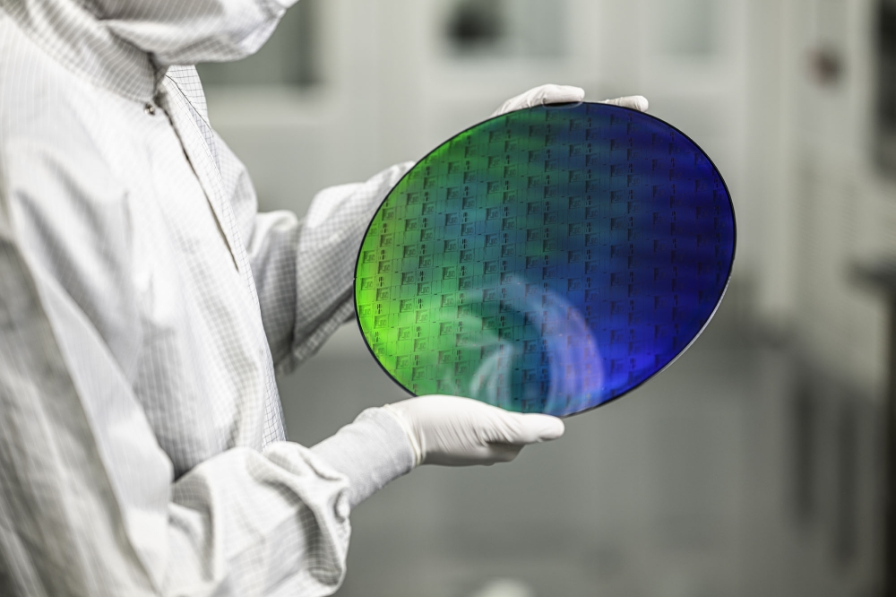
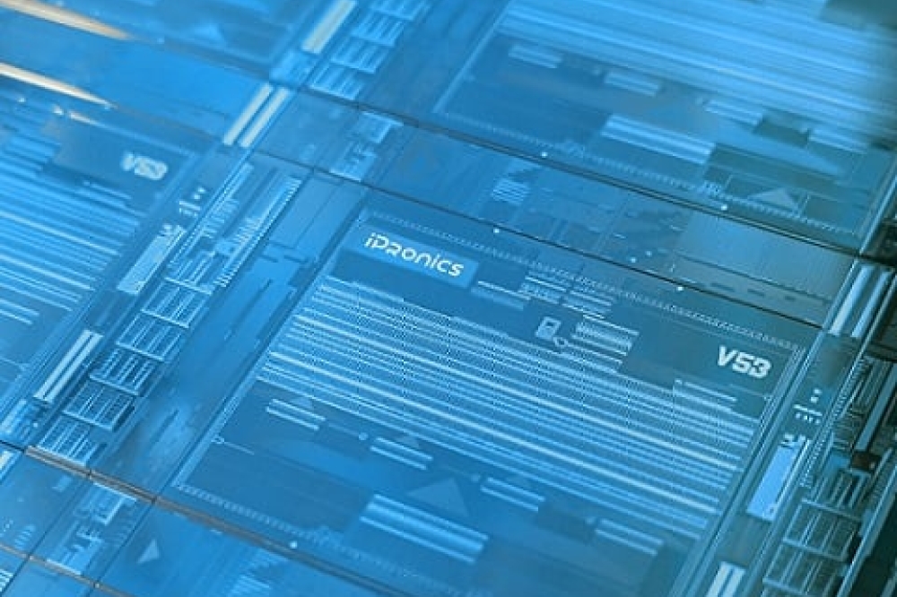
UniversityWafer, a supplier of high-quality semiconductor substrates, has announced the availability of its industry-standard 220 nm device layer silicon-on-insulator (SOI) wafers. The company says these specialised wafers have become the cornerstone of PICs, enabling the development of advanced optical communication systems, data transmission solutions, and next-generation photonic devices.
As datacentres, telecommunications networks, and computing systems strive to increase performance while reducing energy consumption, integrated photonics has emerged as a transformative technology. At the heart of this revolution is the 220 nm device layer SOI wafer – a critical substrate that facilitates the fabrication of compact, high-performance photonic components.
The 220 nm device layer thickness has been established as the industry standard for integrated photonic applications for several compelling reasons, including its ability to support single-mode light propagation in the near-infrared, its high refractive index contrast, low-loss optical transmission, compatibility with CMOS fabrication, and suitability for key photonic components, including ring resonators, Mach-Zehnder interferometers, directional couplers, and grating couplers.
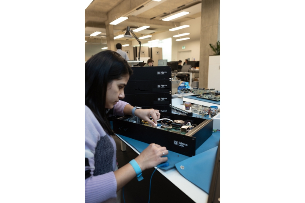
UniversityWafer has been supplying silicon substrates for academic institutions, research laboratories, and industrial manufacturers for over two decades. With a commitment to quality, precision, and customer satisfaction, the company says it is uniquely positioned to support the expanding photonics sector.
“Our 220 nm SOI wafers represent the gold standard for integrated photonic applications,” said a spokesperson for UniversityWafer. “We understand the critical role these substrates play in enabling innovations in optical communication, data processing, and sensing technologies. By providing researchers and manufacturers with reliable, high-quality SOI wafers, we are helping drive the future of photonic integration.”