Creating photonic chips with a laser printer
Researchers have developed a new technique for fabricating rewritable PICs using phase-change materials
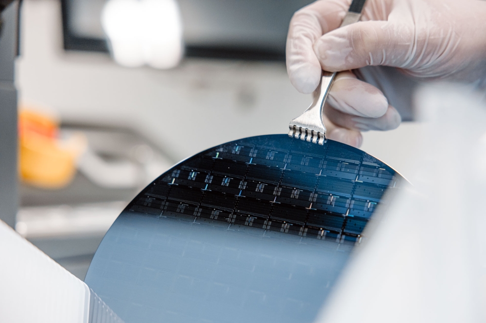
As PICs find applications across a broad spectrum of near-future technologies, from LiDAR and biomedical sensors to 6G and quantum computing, access to fabrication equipment for them is becoming increasingly important. However, today’s nanofabrication facilities cost millions of dollars to construct and are well beyond the reach of many colleges, universities, and research labs. Those who can access a nanofabrication facility must reserve at least a day for the time-consuming lithographic process. Furthermore, if there is a design error, or if the chip doesn’t work properly, it must be discarded, the design adjusted, and a new chip fabricated. This often results in days or even weeks spent in the cleanroom.
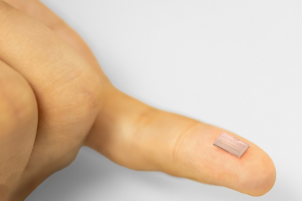
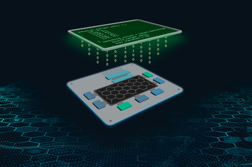
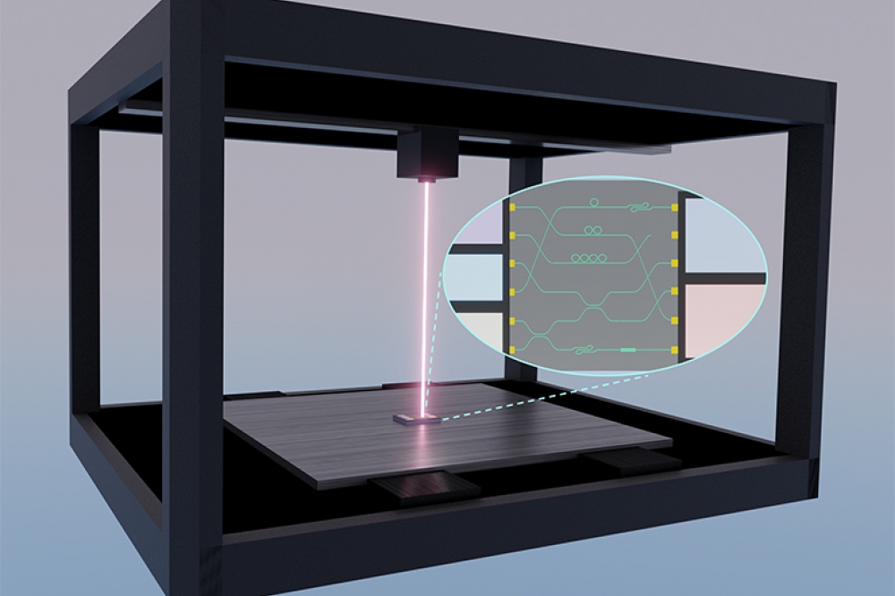
But now, as described in a new paper in Science Advances, a research team led by the University of Washington Department of Electrical and Computer Engineering (UW ECE) has devised a way to bypass expensive nanofabrication facilities and produce PICs almost anywhere. The team has developed an innovative method with which these circuits can be written, erased, and modified by a laser writer into a thin film of phase-change material similar to what is used for recordable CDs and DVDs. With this new process, PICs can be constructed and reconfigured in a fraction of the time it would take at a nanofabrication lab.
The multi-university team was led by Mo Li, a professor of physics and associate chair for research at UW ECE. “Photonics technology is on the horizon; therefore, we need to train or educate our students in this field,” says Li. “But for students to study and have hands-on experience with photonic circuits, currently, they need access to a multimillion-dollar facility. This new technology addresses that problem. Using our method, photonic circuits that previously had to be fabricated in expensive and hard-to-access facilities now can be printed and reconfigured in labs, classrooms, and even garage workshops, by a speedy, low-cost device about the size of a conventional desktop laser printer.”
Researchers can also benefit from this advance, which will enable a much quicker turnaround time for prototyping and testing out a new idea before booking valuable time in a nanofabrication facility. And for industrial applications, a big advantage of this method is reconfigurability. For example, companies could possibly use this technology to create reconfigurable optical connections in datacentres, especially in systems that support artificial intelligence and machine learning, which would reduce costs and boost efficiencies.
Li’s research team included UW ECE graduate student Changming Wu, who is lead author of the paper, and, along with Li, came up with the idea for this novel technique. UW ECE graduate student Haoqin Deng also contributed to the effort. Their work is the latest result of a six-year line of research that includes advances in optical computing. It is also a continuation of a productive collaboration with professors Ichiro Takeuchi and Carlos Ríos Ocampo and their students at the University of Maryland. The work was funded by the Office of Naval Research and the National Science Foundation.
“Being able to write a whole photonic circuit using only one single step, without a complicated fabrication process, is really exciting,” says Wu. “And the fact that we can make any modification to any part of the circuit in our own lab and rewrite and redo it is amazing. It’s a matter of minutes versus a full, day-long process. It’s a huge relief to be able to finish the whole fabrication process within a few minutes instead of what often is several days or even a week.”
The method the team developed has been proven to work, but it is still an early-stage concept. However, Li has filed a provisional patent application, and he is planning to build a desktop laser writer for PICs. The team’s vision is of a laser printer that uses a staging system to move the substrate in a much more precise manner than in a traditional desktop printer, and which can be sold at an affordable price and distributed widely to research labs and educational institutions around the world. The researchers are also looking at reducing optical loss in the phase-change material, to enable the printing of even more detailed and sophisticated circuits.
Li is already engaging with industry leaders to promote possible applications of this new technology in programmable PICs and reconfigurable optical networks. “This technology can create the photonic circuitry you want, but it also can be added onto already-existing electronic circuitry,” he explains. “And because it is reconfigurable and reusable, it just opens many possibilities for students, researchers, and industry. What’s most exciting to me is that we’ll potentially have a huge impact on the field of photonics in disseminating this new tool and technology to the broader research community.”
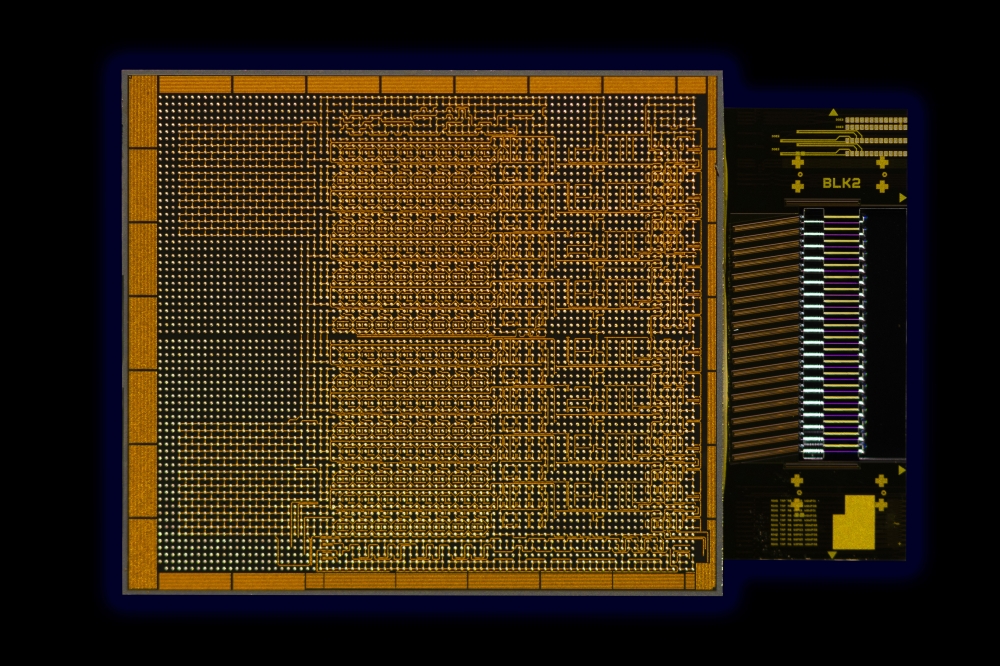
Image credit: Haoqin Deng