
Fraunhofer IPMS developing near-infrared silicon-based photodiodes
The institute has received government funding for the new project, and hopes it will enable new applications with silicon devices, reducing costs and environmental hazards associated with current near-infrared photodiodes
Image sensors and their core component, the photodiode, are indispensable in numerous applications, whether in process, measurement, automotive or safety technology. In the near-infrared range, which is particularly important for many analytical applications, silicon-based photodiodes do not yet offer sufficient sensitivity. Therefore, other materials are used, but they are expensive and sometimes harmful to the environment.
To address this challenge, a new project at the Fraunhofer Institute for Photonic Microsystems (IPMS) aims to develop sensitive silicon-based photodiodes, which are more cost-efficient in production. The Federal Ministry of Education and Research in Germany (BMBF) is funding the MesSi project with €566,000 for a period of three years.
Photodiodes can be found everywhere – as image sensors in cameras inspecting surfaces in process technology or in spectroscopy systems in metrology. In the visible range almost all photodiodes today are made of silicon, as this material is used by default in the semiconductor industry and can therefore be produced more cost-efficiently. However, in the near-infrared range, not visible to the human eye, silicon-based photodiodes have not been used to date, due to their low sensitivity.
For this reason, materials such as indium gallium arsenide (InGaAs) are used in this range. This material requires its own manufacturing processes however, which are not compatible with silicon semiconductor technology and therefore result in high costs. In addition, heavy metals such as arsenic are used in the manufacturing process. This stands in contradiction to efforts to make the production of microelectronics more environmentally friendly.
Fraunhofer IPMS is pursuing a new research approach to help low-cost silicon photodiodes achieve sufficient sensitivity in the near-infrared. “The innovation is based on the implementation of a new structure in our photodiode,” explains project coordinator Michael Müller from Fraunhofer IPMS. “Instead of the usual planar device topography, we use novel pyramidal and ring structures that function like a light collecting basin. With a very thin metal layer in the Schottky barrier, we increase the internal quantum efficiency – meaning the number of charge carriers generated by light in the semiconductor. We think that these two innovations will significantly increase sensitivity and enable near-infrared applications with silicon photodiodes for the first time.”
In the future, silicon photodiodes could enable several new applications in the near-infrared range, particularly in price-sensitive but high-volume markets. One example is autonomous driving, which requires new LiDAR sensors and fog cameras for effective environmental monitoring. This is particularly important when visibility is obstructed by smoke or fog, which causes optical cameras in the visible range to fail.
Security technology would also benefit from this, with applications ranging from the protection of critical infrastructure to the private sector. There are also numerous applications in chemical and medical imaging as well as spectroscopy. Hyperspectral imaging in the near-infrared is used in process measurement technology in the pharmaceutical and chemical industries to detect and analyse organic materials and material mixtures.
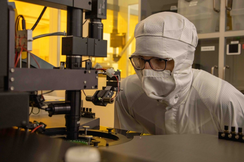
Image credit: Fraunhofer IPMS


