People, planet, profits: a sustainable way forward for all

While pushing the boundaries of technology, businesses increasingly face a critical workforce shortage and pressing environmental responsibilities. A project run by MIT has recently won NSF funding to address these challenges to build a more sustainable future for microchip manufacturing.
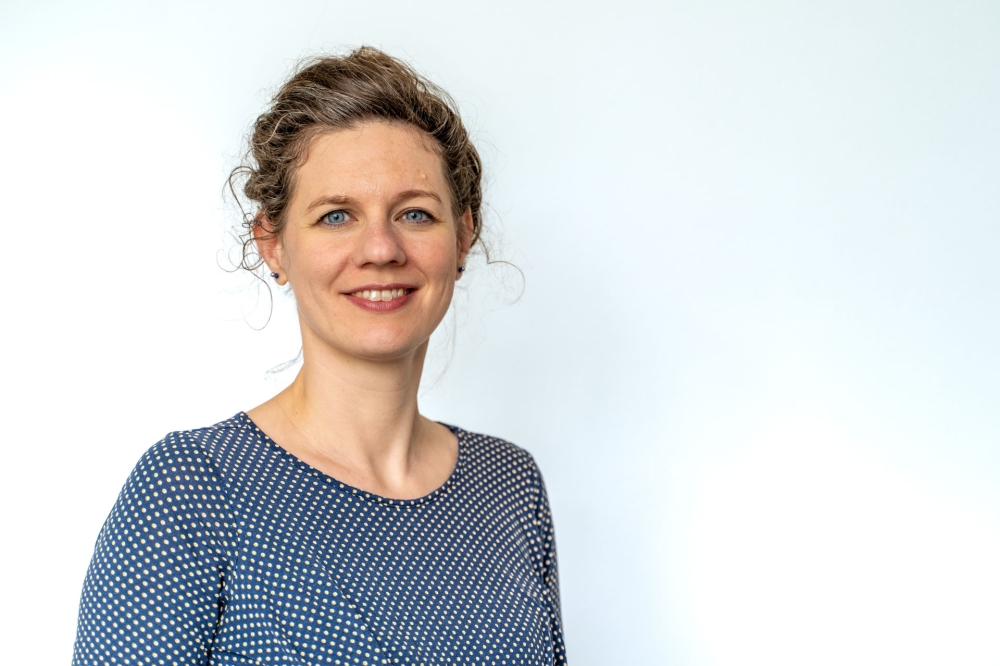
Laura Hiscott, Editor of PIC Magazine interviews Anu Agarwal, principal investigator on the project and principal research scientist at the Microphotonics Center and Materials Research Laboratory of the Massachusetts Institute of Technology (MIT)
LH: Could you tell me a bit about FUTUR-IC? How did the project start and what is its vision?
AA: The project is on microchip manufacturing and sustainability, and we started it when we were funded by Dr. Linda Molnar, Program Director of Track I: Sustainable Materials for Global Challenges. This funding came through the National Science Foundation (NSF) Convergence Accelerator’s Directorate for Technology, Innovation and Partnerships (TIP) in December 2022. As we started to think about sustainable microchip manufacturing, we realised that it is not a simple problem. It’s not just one size fits all. Instead, it’s multiple problems rolled in together. While we were brainstorming and wondering how the future of integrated circuit (IC) manufacturing should look, we realised there were three main branches to think about: technology, ecology, and workforce.
These three dimensions, as we call them, need to be simultaneously optimised. What that means is, we need to enhance microchip performance to meet the future needs for, say, AI, LiDAR, self-driving cars, and quantum applications, but we must think about doing it in an environmentally sustainable fashion. We must educate our workforce so they can meet the STEM performance challenges with sustainability top of mind.
FUTUR-IC will enable the coexistence and co-optimisation of people, which is workforce, planet, which is ecology, and profits, which is technology. But we cannot do it alone within academia. We must be rooted with industry associations, companies, universities, governments, and policymakers. This is the only way we can build a sustainable microchip supply chain for the future of our planet.
LH: After running FUTUR-IC for a year with Phase 1 funding from the NSF, you have now received a Phase 2 Award, which is a clear signal of its value. Did the NSF outline in their decision what they find most important about the project?
AA: The NSF Convergence Accelerator TIP Directorate has always been very clear that a positive impact to society is what they care about. That is important to us as well. Based on that, we conducted stakeholder interviews with at least 100-150 people in different walks of life, including people in companies, consumers of electronics, equipment vendors for the electronics industry, materials vendors, people who design the devices, and people in academia who are innovating in electronics. We interviewed people across the spectrum. We also talked to people in the government and in companies that make defence-related electronics.
Based on this use-inspired research, which we learned during NSF Phase 1, the feedback that we got showed the benefit of FUTUR-IC’s work to people/workforce, planet/ecology, and profits/technology, and could have played a part in NSF’s decision. For example, we didn’t just pull three dimensions out of a hat. They were pointedly given to us by all our interviewees saying: “Yes, it’s important to make technology with the highest performance, but at the same time, looking at what impact it has on the environment while ensuring that the future workforce is trained to design sustainably.”
We learned from companies that they don’t have a large enough pool of STEM-trained workforce to innovate new technology. Today we have about 2 million in this industry’s workforce. By 2030, we need to climb to 3 million, and they must be trained not only in STEM but also in semiconductors and green literacy.
LH: You have previously mentioned that the microchip industry has the potential to be a leader in environmental sustainability. Could you expand on this?
AA: Several industries must consider sustainability during their process and design phases if we are to save our planet. One would think: why worry about the microchip manufacturing industry alone? But if you think harder about this microchip industry, it’s made up of chemists, biologists, physicists, engineers, and computer scientists, with everybody working together in an interdisciplinary fashion driving exponential growth. If we can bring that interdisciplinary expertise to solving sustainability problems, think how wonderful that would be. We could transfer what we learn in the microchip industry to adjacent industries. Why not plant that seed of innovation in the microchip manufacturing industry, and perhaps other industries can also enjoy the fruits?
Another important factor is that the microchip industry is not limited to our cell phones and computers anymore. It is everywhere. It is ubiquitous in home appliances, like washers, dryers, toasters, cookers, and cars. Everything has electronics now. For the Internet of things (IoT) to work, so you can remotely access everything, we need microchips. So chips are expanding their scope and footprint in the world tremendously.
There is another reason why this industry should take a leadership role. Everyone’s trying to use ChatGPT with AI chips, which are known to cause overheating problems in datacentres. If we don’t come up with sustainable solutions now, 10 years down the road we’ll be in deep trouble in terms of energy consumption, heat generation, and electronic and chemical wastage. These are problems that we cannot tackle overnight; we must plan solutions early.
LH: You have spoken about creating sustainable electronic-photonic packaging by being strategic about how we approach different tasks, such as computation and communication. Could you elaborate on this?
AA: It is about managing trade-offs between performance and cost. Following the prediction based on Moore’s law the semiconductor industry has been driven towards smaller transistor dimensions. One reason for shrinking the size is that you can get more chips for a given area, leading to increased revenue, if you can hold down the cost of manufacturing. Also, the shrinking dimension has historically yielded enhanced performance, which is typically measured in the telecommunications industry as an increased bandwidth density with significantly lower power consumption.
To continue along the prediction offered by Moore’s Law, some manufacturers are moving towards 3 nm and smaller process nodes. We may be able to push this dimensional shrink of transistors for another decade or so, but we’re soon reaching the physical size limit. So, what’s next?
Why don’t we think about putting more chips in a package to increase bandwidth? Although more chips per package enables the use of shorter copper traces and lowers heat generation, a trade-off is that it also crowds the copper traces closer together, which can make it harder to dissipate the heat generated. So, we need new packaging designs, materials, and processes.
One way out is electronic-photonic integration through smart packaging. We can use electronics for data computation and photonics for data communication. Photonics, because it offers the possibility of high-speed and large-bandwidth data transmission through low-loss optical waveguides, leading to lower energy use, rather than through lossy long-reach copper traces.
A second benefit of electronic-photonic packaging is that for manufacturing photonic devices you can use mature and more environmentally sustainable process nodes, while maintaining high performance. The leading process nodes can be reserved only for manufacturing electronic devices, because that is a requirement for high-performance computation.
A third benefit is modularity. We can make a modular electronic-photonic package where we have photonic chips and electronic chips, each manufactured with different process nodes, maybe even in different foundries, placed next to each other on a common interposer or substrate. This idea is not new. In fact, in August 2023, at the Hot Chips conference, several large companies, including AMD, Intel, TSMC, and Samsung, decided that manufacturers need to start standardising the package to reduce costs.
We can combine these two ideas to get photonics for communication within a standardised electronic chiplet platform. Large companies have already begun using this combined idea. FUTUR-IC is pushing these ideas forward saying: “let’s get on this standardisation bandwagon where we all use electronics for computation and photonics for communication,” which makes microchip manufacturing more sustainable in terms of materials, processes, and energy.
Another benefit of using photonics for communication is that you can design for chips to be further apart from each other. Spatially separated chips in a package can be disassembled for repair or into separate waste streams at the end of life and recycled more readily for easier material recovery, improving sustainability. This might go against your instinct if you are trying to minimise the size of the overall package, but that is an engineering trade-off between size and modularity.
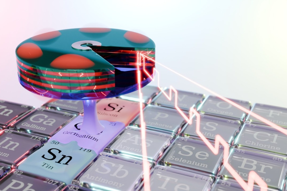
FUTUR-IC is advancing sustainable microchip manufacturing through three dimensions – technology/profits, ecology/planet, and workforce/people. The project has won Phase 2 funding from the National Science Foundation (NSF) Convergence Accelerator’s Directorate for Technology, Innovation and Partnerships (TIP)
LH: It sounds like this can help with several aspects of sustainability?
AA: Yes, photonics helps with sustainability in multiple ways: energy consumption reduction, so less heating of datacentres; more chips per package instead of solely shrinking transistors, so bringing about “More than Moore”; and then this concept of disassembly for repair and into different waste streams. Since we’re in this new era of packaging, why don’t we start with training the workforce to design for sustainability and repair of microchip-containing systems, and to think about this ahead of time, rather than finding out at the end-of-life that repair is too costly or not feasible?
There are several electronic-photonic design automation (EPDA) vendors working on this. For example, Ansys offers software called Granta, which has a sustainable materials database. If I’m designing on Granta, it can tell me: “Hey, I notice that you’re using this particular polymer. Have you considered this other polymer that has the same properties you’re looking for, but is easier to recycle at end-of-life?” Upfront, it’s giving engineers a sustainable alternative. There are other software packages that offer such “Design for Sustainability” options.
FUTUR-IC is introducing lifecycle assessment models for processes across three areas of microchip manufacturing: production, distribution, and use. We are calculating carbon footprints and handprints. Handprinting is the inclusion of the impact of positive environmental actions into lifecycle assessment models. Can we design and make cradle-to-cradle products?
FUTUR-IC has been promoting something called design for repair and upgrade. We all know of the three ‘R’s: reduce, reuse, recycle. But we’re adding another ‘R’, for repair, and a ‘U’, which is upgrade. Let us try to repair our electronics. Let us try to upgrade our devices by just replacing one chip as opposed to throwing the entire device or appliance away.
LH: You mentioned that several companies at Hot Chips 2023 highlighted the importance of standardisation. What needs to happen for the industry to collectively move in this direction?
AA: Everybody must get on board. There must be a movement. Standardisation happens when everyone agrees that there should be standards. For example, if people decide that there should be a standard universal charger for cell phones, no matter the company, make, or model, it will happen.
FUTUR-IC is promoting electronic-photonic packaging, standardisation,
and modularity, as practices that can make the microchip manufacturing
industry more sustainable. Adapted with permission from Drew Weninger et
al., “High density vertical optical interconnects for passive
assembly,” Opt. Express 31, 2816-2832 (2023) © Optica Publishing Group
Other standardisation approaches relate to what I was saying about packaging. Let’s say I need a way to put together an AI accelerator chip, a memory chip, and another chip that does my specialised custom function. How can I put it all together without having to redesign a package from scratch for each product? And it’s not only good for the environment, but also good for the companies, as it becomes easier and less expensive for them to source components with a mix-and-match approach.
We’ve interviewed about 140 companies, and what they said to us is that technology drives the business, but ecology maintains business continuity, because, for example, if the planet runs out of lithium there can be no business. And finally, workforce grows the business. Without a well-educated workforce, not just in STEM (science, technology, engineering, and mathematics), but also in sustainability, we cannot grow in the right direction. So that’s why we need to co-optimise the technology, ecology, and workforce dimensions. There are lots of companies and groups doing one or another. But FUTUR-IC works on them simultaneously.
LH: You mentioned that tech companies are facing a shortage of people with the appropriate technical skills. How is MIT working to address this issue?
AA: There is a huge workforce shortage, not just in the US, but globally. Anecdotally, people have been saying that students used to come to their professors as they were getting close to graduation, asking for recommendation letters for jobs. Now, students are coming in and saying: “I have five job offers and I just have to pick one – no thank you, I don’t need a recommendation letter!”
At MIT, our team is building a roadmap for microchip technology as well as for the semiconductor workforce. Through a different programme, members on our team are creating a Workforce Readiness Level (WRL) categorisation, just like we have the Manufacturing Readiness Level (MRL). Our philosophy at MIT has been agile continuous education using a three-legged stool approach. The first leg is lectures, or some kind of pedagogical teaching, with which we are all very familiar. The second leg is Virtual Reality (VR) simulations to build intuition. And finally, the third leg is hands-on training in labs, for which the Commonwealth of Massachusetts has invested about $18 million into five LEAPs (Lab for Education and Application Prototypes) across the state (cam.masstech.org/cam-programs/lab-education-application-prototype-leap).
In terms of traditional education, we have teaching packages, short courses, and a summer academy. We also have several online electronics, photonics, and sustainability courses available.
We have a virtual lab photonic device simulation library which you can find on the website of our partner AIM Photonics (www.aimphotonics.com/simulation-library), with simulations of photonic device components, such as a Y-branch splitter, Mach-Zehnder interferometer, ring resonator and others. One simulation, for example, shows you how light bends at corners. You can see that there’s loss at an edge with a sharp bend, and if you change the radius of curvature to be less sharp, there’s less loss. This is what I mean by building intuition.
The simulation for a directional coupler shows you what happens when you bring two waveguides close to each other, or if you change the length of the coupling region. If you look at the output, you can see whether the modes couple from one waveguide to the other, depending on the coupler length and the wavelength. We’ve created these browser simulations based on solutions to Maxwell’s equations.
FUTUR-IC is working on many educational initiatives for workforce
training and development, including a library of simulations that build
intuition around how light behaves within various photonic components.
A learner may ask: what happens if I change the radius of my device? What happens if I change the gap between these waveguides? What happens if I move from one wavelength to another? The VR simulations provide them with an immediate intuitive understanding of the behaviour of light in on-chip devices.
For practical training, we have hands-on bootcamps that we offer at MIT and with Professor Samuel Serna at Bridgewater State University, which is a four-year college in Massachusetts. Through an NSF-ATE programme led by Suny-Poly in New York and MassBay Community College in Massachusetts, we offer bootcamps to students in community colleges and help to place them in company internships following the training. With bootcamps, apprenticeships and internships, we bring people into labs, and we teach them how to perform hands-on testing. We are hoping that this successful three-legged stool education model can be replicated across the country.
We have an education team at MIT within the Initiative for Knowledge and Innovation in Manufacturing (IKIM), and you can see all our educational offerings at ikim.mit.edu. Our education director is Dr. Sajan Saini, and Professor Lionel Kimerling leads IKIM. Due to this IKIM team effort in education and workforce development over the last five years, we stand where we are today.
LH: The Phase 1 Award was for a year, but the Phase 2 Award is for three years. Will this enable the FUTUR-IC team to do anything qualitatively different, or is the main outcome the further continuation of the research?
AA: The longevity helps in goal setting. We know what we want to accomplish in the long term – a sustainable microchip industry. In the short term, we’re working with low-volume foundries, and eventually we’ll go to higher-volume foundries, packaging houses, and design vendors. Now the fact that we have two and a half to three years to work it out means we can start to build our relationships with the various stakeholders, gather the data that is required, and then build technology, ecology, and workforce products, and co-optimise them simultaneously. It gives us some more flexibility because it’s over a longer period and we have time to course correct whenever necessary.
The result should be the same, which is sustainable microchip manufacturing across the supply chain. But how we apportion the tasks that we’re doing, our deliverables, is different. They are broken down according to what should be done in year one in order to build for year two and year three.
LH: The MIT Microphotonics Center is also co-leading the Integrated Photonics Systems Roadmap-International (IPSR-I), together with PhotonDelta from the Netherlands. How can companies and research institutes get involved?
AA: The IPSR-I started out as a communications technology roadmapping initiative, and it’s now an international project. We have partnerships from Japan and Europe, and we have partnership requests coming in from South America as well.
We have two meetings a year. One is in June at MIT, and one is in autumn in Eindhoven. There’s a lot of interest in the technology roadmap. Anyone interested in joining is welcome to reach out to us (at anu@mit.edu) or go to our website, ikim.mit.edu, and ask what they can do to move the sustainability needle in the right direction by simultaneously benefiting people, planet and profits.


