Harnessing InP for applications beyond optical communications

Photonic chips are well established in optical communications markets. However, InP PICs are now proving versatile, as they are increasingly adapted to unlock other applications, from AI and neuromorphic computing to quantum technology and sensing.
By Paul Momtahan, Director of Solution Marketing, Infinera
Since its inception several decades ago, photonic integration technology has delivered a plethora of benefits, which have so far been reaped largely by the telecom industry. Fundamentally, PICs perform multiple photonic functions on a single chip, as outlined in Figure 1. As is the case with conventional electronics, manufacturing one high-function chip is far more cost-effective than manufacturing lots of individual optical components and then integrating and packaging them.
Additionally, by enabling device miniaturisation, photonic integration can dramatically reduce footprint, exemplified by the evolution from large coherent transponder modules to compact digital coherent pluggables in a wide range of small form factors. PICs also offer reduced power consumption, as well as improved performance due to minimised coupling losses when connecting photonic functions with waveguides inside the PIC, as opposed to coupling optics between discrete components. Since these external coupling losses are eliminated as a source of failure, equipment failures, too, are less frequent.
Having proven their value in the telecom industry, PICs are now also being explored as a potential enabling technology in a wide range of other fields. From AI and neuromorphic computing to quantum technology and sensing, integrated photonics – and the indium phosphide platform in particular – is a versatile tool that could supercharge the development of numerous transformative applications.
Figure 1: Benefits of photonic integration for optical communications.
A brief history of PICs
The concept of combining multiple optical components in a single circuit has been around for 55 years, since Stewart Miller of Bell Labs published a paper called “Integrated optics: An introduction” in 1969 [1]. This paper proposed a PIC consisting of a single integrated laser and modulator and suggested that savings would result from the use of photonic integration.
Then, in 1987 two papers further described integrating a laser and a modulator, one by researchers at KDD Research & Development Laboratories in Japan [2], and the other by a team at NTT Electrical Communication Laboratories [3]. The latter demonstrated an electro-absorption-modulated laser (EML) in a monolithic indium phosphide (InP) PIC, though these were only successfully commercially deployed later, in 1995.
In 1988, Bookham Technologies, now part of Lumentum, was founded in the UK and went on to become the first company to make optical components that could be incorporated into silicon integrated circuits. In the early 1990s, Meint Smit at Delft University of Technology started pioneering in the field of integrated photonics and is credited with inventing the arrayed waveguide grating (AWG). In 1986, Richard Soref and Joseph Lorenzo published their seminal paper: “All-silicon active and passive guided-wave components for λ = 1.3 and 1.6 µm” [4].
Infinera, founded in 2000 as Zepton Networks, released its first products leveraging the industry’s first large-scale monolithic PICs in 2004. These PICs, one for transmit and one for receive, integrated all the components for the transmitter and receiver respectively for 10 x 10G direct-detect wavelengths in a single monolithic device. Combined with Infinera’s optical transport network (OTN) switching technology in the delay-tolerant networking (DTN) product, these PICs transformed the economics of long-haul transport by addressing the challenge of expensive optical-electrical-optical (OEO) conversion and regeneration.
Infinera selected InP as the material for its PICs because it can support a wide range of functions, including laser and optical amplification at dense wavelength-division multiplexing (DWDM) wavelengths, i.e. the C-band (1529-1567 nm) and the L-band (1569-1610 nm). An additional advantage that has become increasingly important is its inherently superior modulation effect compared to silicon [5], which is especially valuable for the highest-performance segment of the DWDM transceiver market as baud rates evolve to 200 GBaud and beyond.
Metro, long-haul, and submarine
Photonic technology plays a critical role in optical communications, supporting the transmission of tens of terabits per second over the submarine and long-haul terrestrial fibres that form the backbone of the internet, while also facilitating high-speed metro, mobile backhaul, and broadband access networks. Specifically, these metro, long-haul, and submarine networks are powered by coherent optical engines, which incorporate multiple components and functions, including the digital application-specific integrated circuit (ASIC), often referred to simply as the digital signal processor (DSP), an analogue ASIC that integrates multiple drivers and transimpedance amplifiers (TIAs), and the photonics.
The photonic components in the coherent optical engines include the laser that generates light with the desired wavelength and a modulator that takes the light from the laser and encodes the data by changing the phase and amplitude. The coherent modulator itself encompasses four individual Mach-Zehnder modulators (MZMs), as well as beam splitters, combiners, phase shifters, a polarisation rotator, and a polarisation beam combiner. The receive side, meanwhile, has photodetectors and passive photonics, including a polarisation beam splitter and 90 degree hybrid coupler. Infinera’s coherent InP PICs integrate all the transmit and receive photonic functions for one, two, or even six wavelengths on a single PIC.
The PICs that are indispensable in today’s communications networks show that integrated photonics has come a long way in the decades since it was first conceived. But the telecoms industry is only the start; this sophisticated technology can be adapted for use in a wide array of other systems, potentially helping to realise game-changing new applications and accelerate them to market.
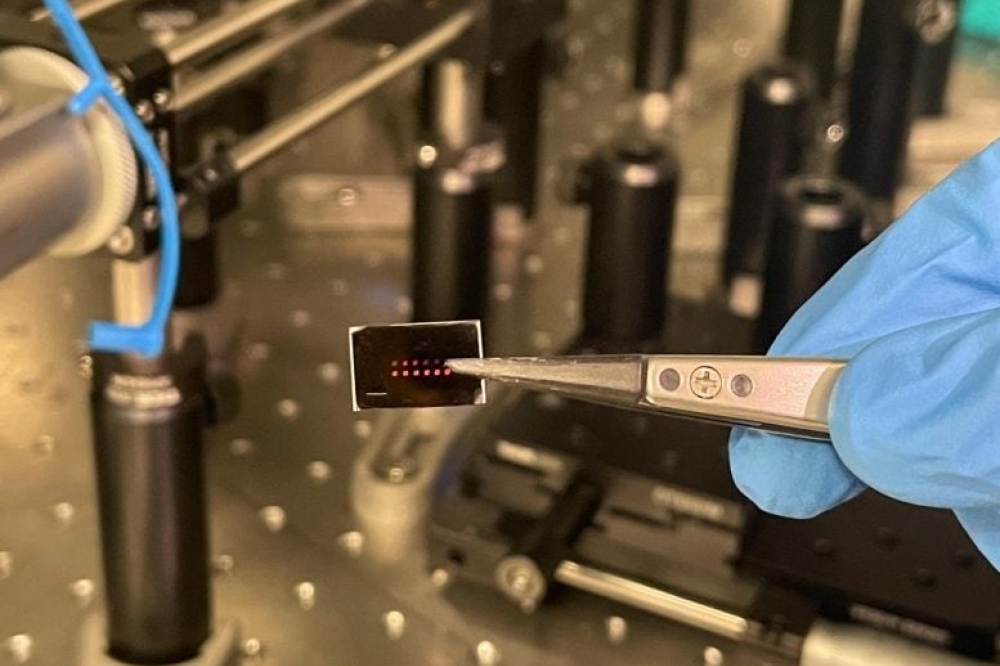
Figure 2: Infinera’s first large-scale monolithic PICs, released in
2024. 10 x 10G transmitter PIC (left) and 10 x 10G receiver PIC (right).
AI datacentres and neuromorphic computing
Generative artificial intelligence (AI) is having a huge impact on the world, not only in terms of how people are using it in their daily lives, but also in terms of the demands placed on the datacentres that provide access to it. There is currently a mismatch between the growth rate of generative AI models and that of the infrastructure they require. In two years, the number of parameters in these models scales by a factor of 100, and the GPUs they run on increase their performance by a factor of 3.3. Meanwhile, in the same two-year period, interconnect bandwidth increases by a factor of just 1.4. In other words, the growth of AI models is currently outpacing the growth of data transfer capacity it requires.
GPU clusters for generative AI are currently scaling by a factor of 10 every three years, with the present state of the art being 32,000 GPUs in a cluster. These clusters will require massive amounts of optical interconnects, with low power and low latency both being critical. Leveraging the low power requirements of InP modulators, low loss of InP, and ability to integrate gain functions including lasers and semiconductor optical amplifiers (SOAs), monolithic InP PICs provide an ideal-material platform for high-speed intra-datacentre optics.
PICs such as Infinera’s newly announced ICE-D products can integrate optical functions including distributed feedback (DFB) lasers and arrays, ultra-low-voltage MZMs, low-switching-voltage electro-absorption modulators, and photodiode arrays, making them a compelling option for scaling intra-datacentre optics to 1.6T, 3.2T, and beyond.
Furthermore, these versatile InP PICs can be used with a variety of different optical setups. For example, they are compatible with today’s retimed pluggable optics (RPO), which have DSP functions for transmit and receive, as well as new industry initiatives such as linear-drive pluggable optics (LPO), which remove the DSP from the pluggable optics. They can also be used with pluggables that that have a DSP function only for transmit, referred to as linear receive optics (LRO) or half-retimed linear optics (HALO), and co-packaged optics (CPO), which replace pluggable optics with optics packaged with the switching silicon.
Another way in which InP PICs could advance AI and machine learning (ML) is through the field of neuromorphic computing. This area of research seeks to build computer chips with neural networks embedded in the hardware itself, as opposed to running neural network software on conventional processors.
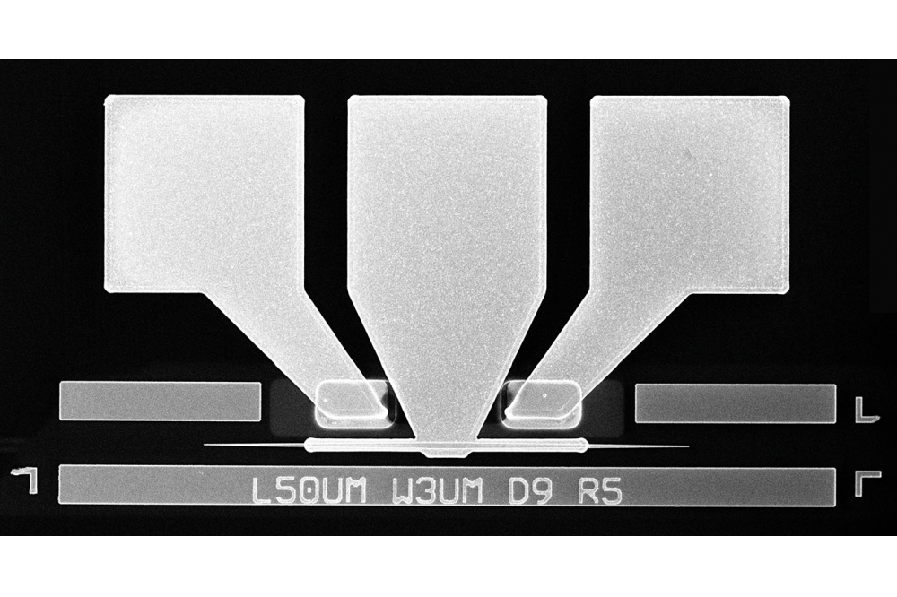
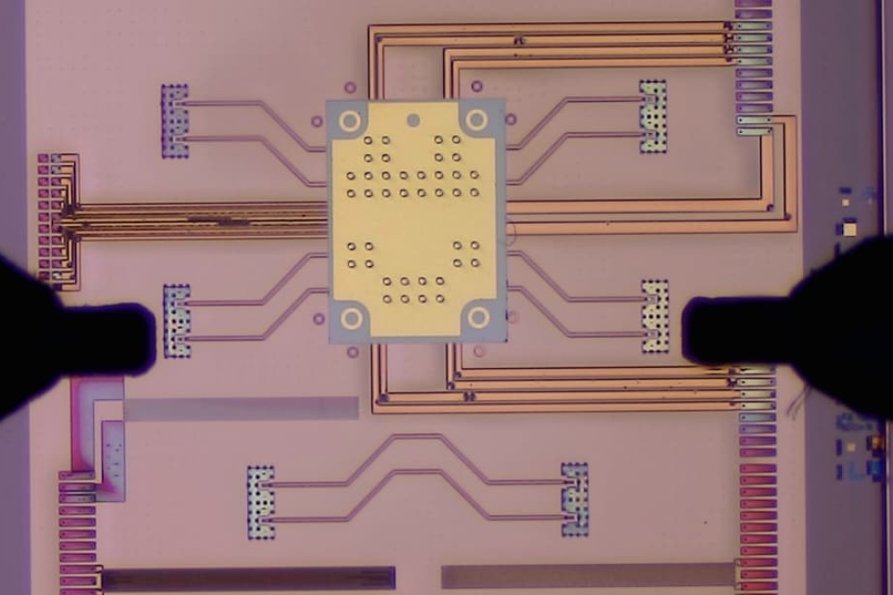
Internally, these chips require massively parallel interconnections, making InP PICs a strong candidate, with optical waveguides replacing the metallic interconnects in an electronic integrated circuit. Eindhoven University of Technology demonstrated this type of device in 2020 with an InP PIC as shown in Figure 2 [6]. As the field evolves, photonic neuromorphic processors could become a key enabling technology to harness the power of AI/ML for wide-ranging applications, including high-energy particle physics, fusion reactor control, and nonlinear optimisation for robotics and autonomous vehicles.
Figure 3: InP PIC for photonic neuromorphic computing (Eindhoven University of Technology, 2020)
Quantum tech and photonic sensing
Another area getting a lot of attention and investment is the field of quantum technology. Since InP’s properties enable quantum effects at the individual photon level, PICs based on this material could be a key technology in achieving the exciting goals of the quantum revolution. For example, InP colloidal quantum dots could be a less toxic alternative to today’s cadmium-based quantum dots for use as single-photon sources.
Meanwhile, researchers are also investigating the material’s potential for use in quantum-safe cryptography. Quside, a startup based in Barcelona, Spain, has developed a high-performance random number generator based on an InP PIC that has tremendous potential as an enabler for quantum-safe encryption. This random number generator could also facilitate faster and more energy-efficient simulations, which are needed to produce, for example, weather forecasts and risk analyses in the financial sector.
Yet another key emerging application for InP PICs is sensing. The material is already used for short-wave infrared (SWIR) sensors and edge-emitting laser (EEL) proximity sensors; the third generation of Apple AirPods were the first device to leverage InP SWIRs in 2021, while the iPhone 14 Pro was the first to use an InP EEL. 3D sensing in smartphones and tablets, which is used for applications including facial recognition, currently uses gallium arsenide (GaAs) vertical-cavity surface-emitting laser (VCSEL) arrays. However, this is also expected to evolve to InP, as the notch in the phone shrinks to a dot. This is because InP-generated light at 1310 nm can pass through the OLED screen transparently, unlike GaAs-generated light, which is in the range of 780-980 nm.
In the area of automotive LiDAR, moving to InP offers another advantage over today’s GaAs-based solutions; since InP-generated light can operate in the mid-infrared range, it can offer higher laser power without posing a risk to pedestrian eye safety, unlike the near-infrared range of incumbent GaAs-based LiDAR. The material can thus facilitate longer ranges of more than 200 m. Moreover, InP LiDAR can leverage frequency-modulated continuous wave (FMCW), rather than today’s time-of-flight (TOF) techniques. Whereas the latter measures only the distance and direction of detected objects, the former also measures their velocity, enhancing accuracy and safety.
Finally, the mid-infrared frequency range can also be applied to medical use cases. For instance, it could expand the monitoring capabilities of wearables like smart watches to include blood markers such as glucose, lactate, and alcohol.
All these examples offer a glimpse into the myriad fields that InP PICs are now flourishing in. Although they have so far primarily been developed for telecoms, underpinning the coherent transceivers used in communications networks, their potential is increasingly being tapped for diverse and potentially world-changing technologies. As we strive towards a future with larger generative AI datacentres, new computing paradigms, quantum cryptography, safe autonomous vehicles, and non-invasive medical monitoring, InP PICs may be an essential part of helping us get there.


