Going Vertical to Advance PICs
ECE Prof. John Bowers and his lab researchers have spent
several decades advancing photonic integrated circuits (PICs) – and now, with
Caltech and Anello photonic colleagues, they have achieved a significant
breakthrough
Bowers and the researchers' work appears in the August 3 issue of the journal NATURE, in an article titled “3D integration enables ultralow-noise isolator-free lasers in silicon photonics.”
“We have been collaborating with Caltech and Anello Photonics to reduce the noise in lasers and photonic integrated circuits by significant amounts, sometimes a factor of 1 million,” says Bowers. “This is achieved by added functionality in the photonic integrated circuit, which enables compact, integrated devices to exceed the performance of bulky optical systems.”
Lead author, Chao Xiang, who earned his PhD in Bowers’s lab in 2021, continued as a postdoctoral researcher to finish this work, and is now an assistant professor at the University of Hong Kong, notes, “The performance and functionality of the PIC described in this paper are much better than what has been achieved previously,” adding, “The biggest finding is that the new 3D integrated architecture allows us to combine the best of the two types of photonics devices: active and passive. Lasers are active in that they require an electrical current to be injected to operate and produce light. A waveguide, used to convey the laser output, is passive, as it requires no external control to function. In our architecture, the passive element is on the bottom, and the active element is on top, allowing each to perform optimally on a single wafer. That’s a very important part of this work.”
Xiang adds that, while 3D integration is not an entirely new theme in photonics, “No one had ever made it this complicated. Maybe people thought about something like this but could not quite make it happen. The experience and knowledge with heterogeneous integration in John’s group made it possible to achieve 3D integration of lasers with ultra-low-loss waveguides.”
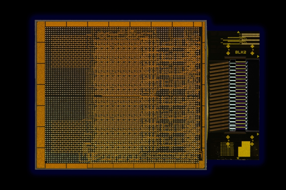
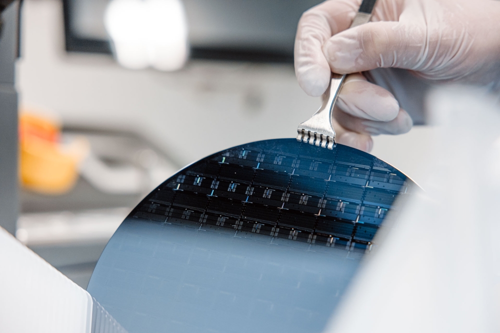
The new 3D architecture, Xiang explains, has many layers, both monolithic and heterogeneous. In monolithic architecture, all of the materials are on the same substrate, while in heterogeneous architecture, different substrates are bonded together. “It’s perhaps the most complex PIC to date,” Xiang says, “and while complexity is not desirable in and of itself, the architecture has to be complicated in order to combine the various functionalities on a chip that can be produced in a CMOS [complementary metal-oxide semiconductor] fabrication facility. It’s definitely the cutting edge.”
The authors note that, while photonic integrated circuits are widely used in applications such as telecommunications and datacenter interconnects, they are still considered inferior in microwave synthesizers, optical gyroscopes, and atomic clocks. For PICs to replace bulk optics and fibers in those such high-precision applications will require a highly coherent, ultra-low-noise (ULN) laser to be integrated with other photonic components on a single chip.”
Until now, they add, two major obstacles have prevented such a PIC from being made: 1) the high noise of semiconductor lasers (a noisy laser does not emit light at stable frequencies, which is required in high-precision applications) and 2) the difficulty of integrating optical isolators directly on chip. The authors describe overcoming those challenges by introducing 3D integration to produce an ultralow-noise laser that, importantly, does not require an isolator.
An isolator is an indispensable element in a normal laser, which is highly sensitive to light refracting back from downstream, says Xiang. In most cases, only with the protection of an isolator, which blocks such back-refracting light, can the laser function with the necessary level of stability.
A problem arises, however, from the fact that making isolators not only is difficult, but also requires a process that is not compatible with CMOS fabrication. That’s because industry-standard optical isolators are made with magnetic materials, which can contaminate equipment in a CMOS facility. Isolators are, therefore, made elsewhere, which necessitates additional packaging, an impediment to scaling production of integrated on-chip lasers.
Xiang and other researchers in the Bowers group were able to overcome the above-mentioned obstacles by combining a laser with a high-quality-factor, or “high-Q,” silicon nitride ring resonator, which makes the laser insensitive to any refracted photons. The result, Xiang says: “Even if you have very strong refraction, the laser will still work at the same level it would with an isolator. The refraction is still there, but the high-Q ring makes the laser much more stable and robust against it.”
Another challenge was that the active device — the ULN laser — can be made only from a III-V material stack, in this case, indium phosphide. The passive element, however — the ring resonator — has to be made on silicon nitride (SiN). Using the above- mentioned monolithic and heterogeneous processing sequences enabled direct on-chip integration of a laser leveraging a III-V gain medium and ultralow-loss (ULL) silicon nitride waveguides.
The ring resonator serves the crucial function of ensuring what is called long photon lifetime, which, in turn, makes the laser stable and quiet. The photons from the laser go into the ring, where they travel without much dissipation, thanks to the low-loss silicon nitride. Achieving that combination of III-V, silicon, and silicon nitride requires what Xiang describes as “a very complicated fabrication process.”
It begins with the monolithic process, with etching and lithography performed to create one layer. After another layer of materials is deposited on top of that, more lithography and etching are done to form the redistribution layer structure, which controls the coupling between the top III-V/Si layers and the silicon nitride low-loss layers on the bottom. Xiang notes, “It’s a very important layer, because it acts as a bridge that couples the material that is good for active elements [the laser] and the one that is good for passive elements [the ring resonator].”
After that, Xiang introduces another two-layer substrate, including silicon and indium phosphide, and uses wafer bonding to make the whole heterogeneous package.
3D integration is the key to making the laser-ring resonator function well, because it creates enough distance between the laser and the resonator so that they don’t interfere with each other and also prevents any impurity from being introduced into the bottom, ultra-low-loss material during processes such as etching, thus ensuring stable performance.
Integrating a laser with a very high-Q factor ring resonator on the same chip is especially challenging, Xiang says, because “The indium phosphide used for the laser and the silicon nitride used for the resonator are completely different materials that have fabrication-process incompatibilities, and you have to work around those to make the materials work together on the same wafer substrate. We were able to find an architecture that allows both materials to work optimally at the same time.”
Having overcome the extreme challenge of integrating III-V materials with silicon via heterogeneous integration, Bowers notes, “We are now making a much better laser. Integrating the low noise laser with modulators and photodetectors enables integrated transceivers, LiDARs, gyroscopes, sensors, and other new applications.”
From the COE News – "Going Vertical to Advance a New Realm of High-Precision PICs"
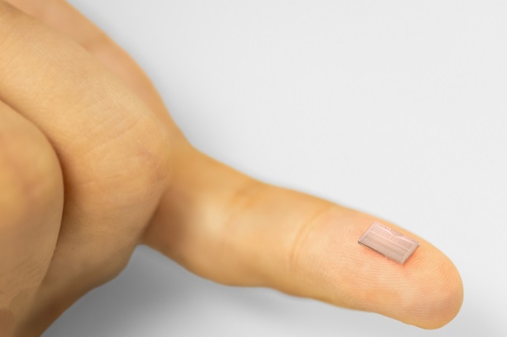
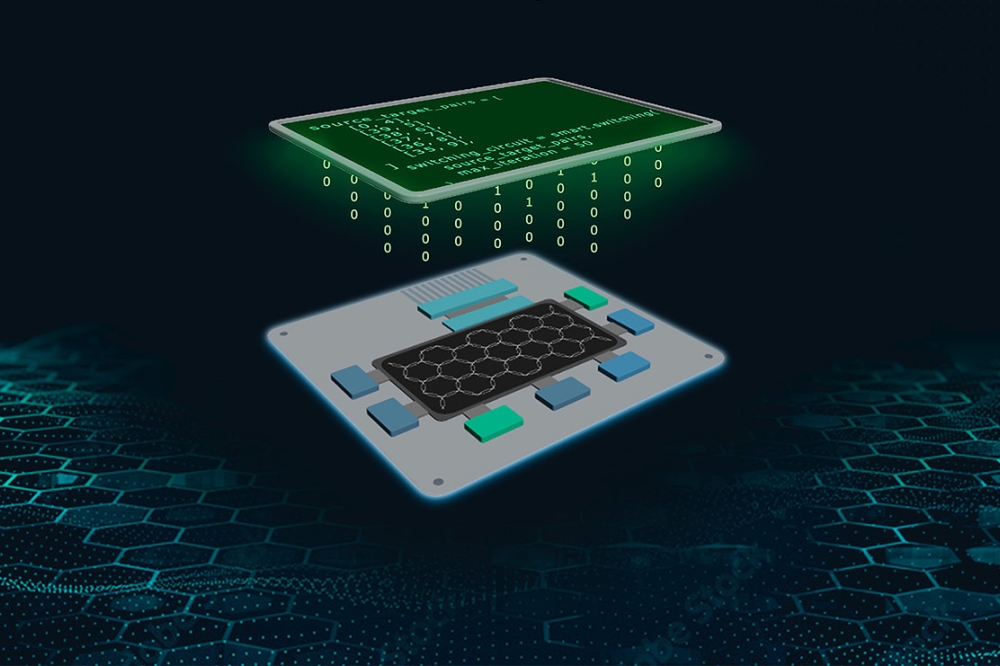
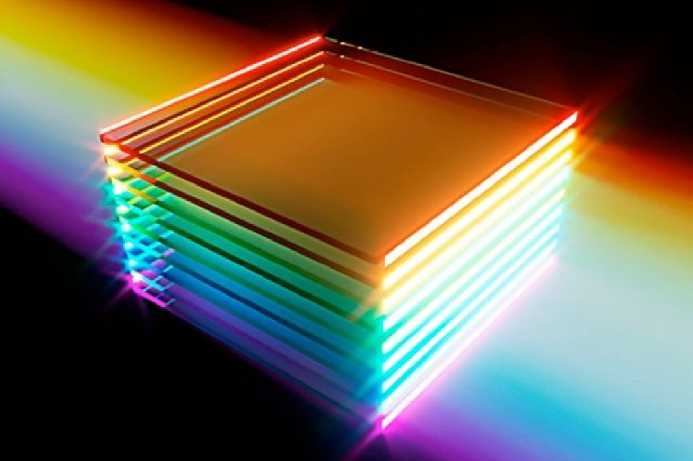
Illustration: Artist's concept illustration depicting a stack of heterogenous materials similar those used in this project.