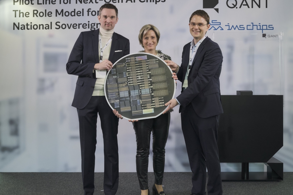
Q.ANT and IMS CHIPS launch production line for photonic chips for AI
The company is repurposing the existing facility at the Institute of Microelectronics Stuttgart to produce high-performance, energy-efficient TFLN-based photonic processors, marking a significant semiconductor manufacturing milestone
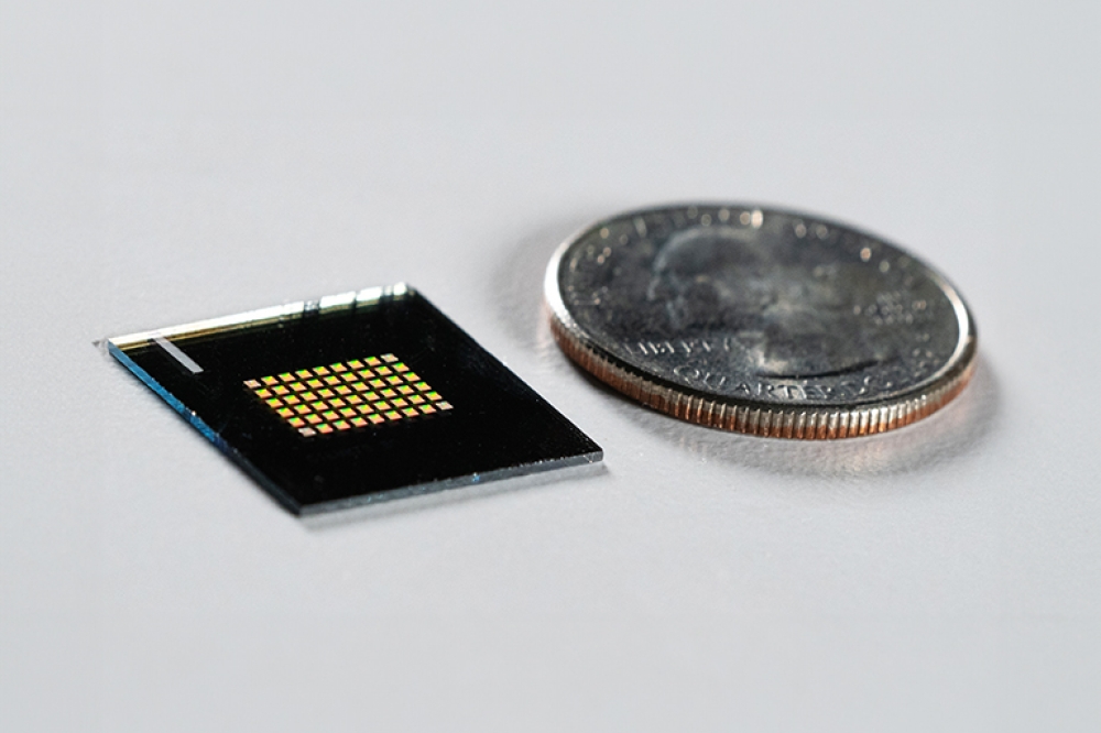
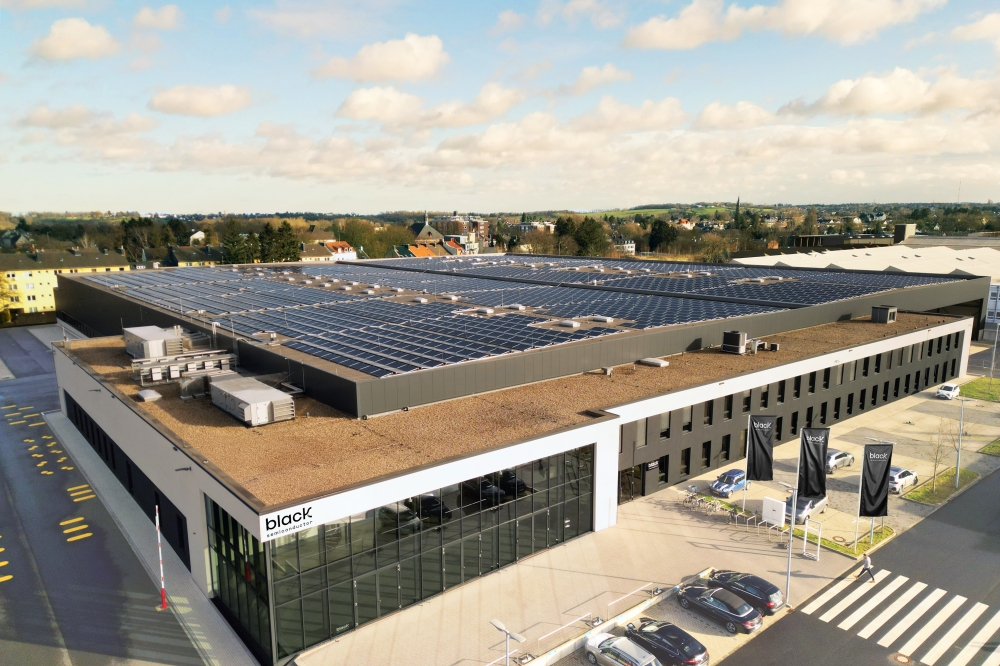
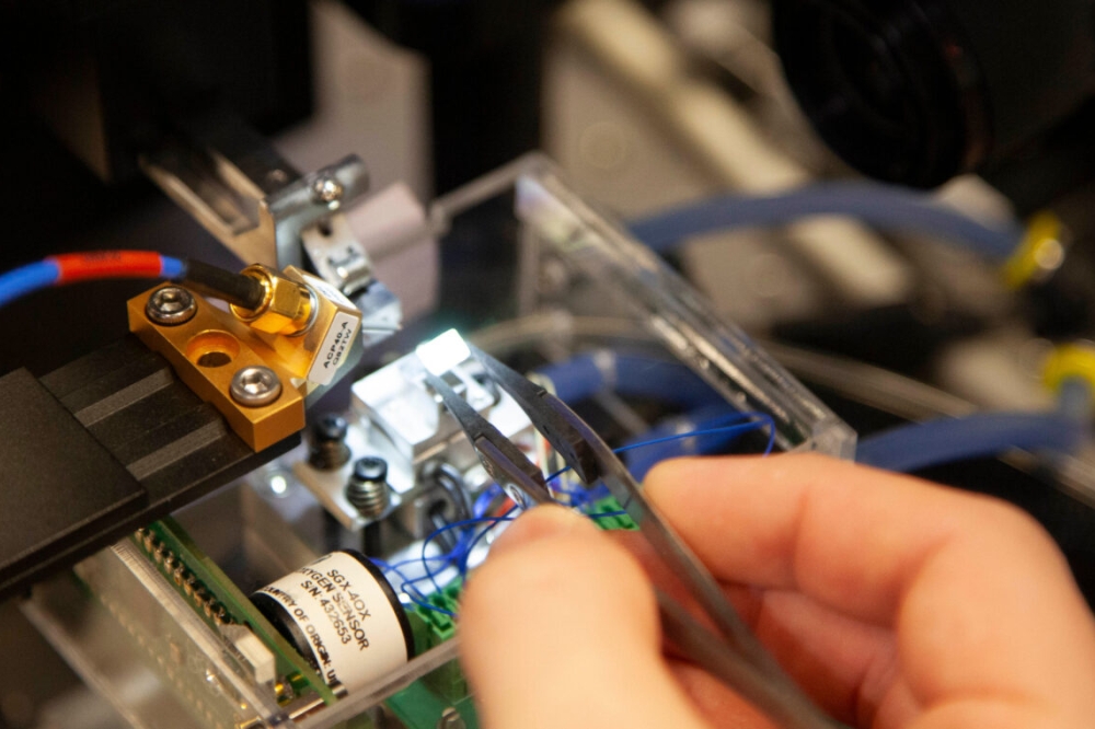
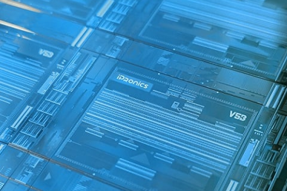
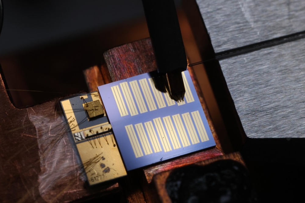
Q.ANT, a company focusing on photonic processing for AI, has announced the launch of a dedicated production line for its high-performance photonic AI chips at the Institute of Microelectronics Stuttgart (IMS CHIPS). By integrating Q.ANT’s patented photonic chip technology on the base of thin-film lithium niobate (TFLN) and upcycling the existing CMOS production facility, Q.ANT and IMS CHIPS say they have established a first-of-its-kind manufacturing line to accelerate the production of energy-efficient, high-performance processors for AI applications. Q.ANT has invested €14 million in machinery and equipment to complement the new line.
According to the company, this manufacturing approach delivers faster, more energy-efficient processors to meet the growing computational demands of AI and high-performance computing (HPC), while also establishing a blueprint for cost-effectively modernising chip production worldwide, and for democratising production capacity. It aims to enable countries to attain greater semiconductor manufacturing resilience, reduce dependency on global supply chains, and accelerate the development of critical technologies that drive innovation across datacentres, research institutions, and advanced industries.
The official launch event, attended by leading industry figures and German officials, underscored the project’s significance in driving innovation within the European and global semiconductor ecosystem. By modernising existing chip production capabilities, Q.ANT and IMS CHIPS say they have pioneered a scalable approach to bringing energy-efficient AI processors to the market at a faster pace, more cost-effectively, and more sustainably.
Q.ANT’s photonic chips – which compute using light instead of electricity – deliver a 30-fold increase in energy efficiency and a 50-fold boost in computing speed, offering transformative potential for AI-driven datacentres and HPC environments, the company says. The pilot line is specifically designed for production using TFLN, the optimal material for photonic computing and critical to the success of the technology. TFLN enables ultra-fast optical signal manipulation at several GHz without the need for heat to modulate the light on the photonic circuit. This advantage leads to more precise and energy-efficient control of the light, resulting in a significant increase in computing power and energy efficiency compared to traditional silicon.
“This approach establishes a new benchmark for AI chip manufacturing, providing a path towards greater self-sufficiency and more energy-efficient chip solutions,” says Michael Förtsch, CEO of Q.ANT. “As AI and data-intensive applications push conventional semiconductor technology to its limits, we need to rethink the way we approach computing at the core. Q.ANT is driving this shift with photonic computing to achieve unprecedented energy efficiency and computational density. With this pilot line, we are accelerating time to market and laying the foundation for photonic processors to become standard coprocessors in high-performance computing. This milestone marks a major step toward the future of sustainable AI chip technology, engineered and produced in Germany for a rapidly evolving global market. By 2030, we aim to make our photonic processors a scalable, energy-efficient cornerstone of AI infrastructure.”
Jens Anders, director and CEO of IMS CHIPS, said: “This pilot line at IMS CHIPS demonstrates how transformative technologies can thrive on existing infrastructure, setting a blueprint for energy-efficient next-generation computing. This comes at a critical time for the computing industry, as the exponential growth of AI and data-intensive applications will soon overwhelm the current datacentre infrastructure. By partnering with Q.ANT, we are leveraging our semiconductor manufacturing expertise to accelerate the industrialisation of photonic processors and establish a scalable model for energy-efficient computing – a crucial step for the future of AI.”
Pilot line for greater autonomy and rapid market launch
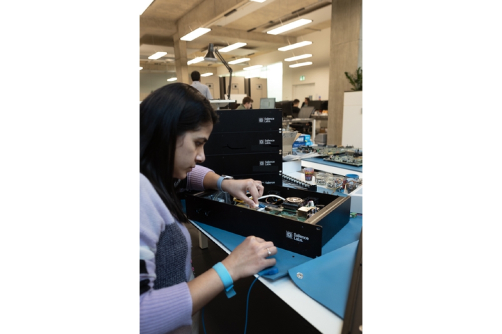
Capable of producing up to 1000 wafers per year, Q.ANT says the pilot line enables it to refine its chip architecture to meet evolving market requirements. It also serves as the R&D basis for the company’s photonic Native Processing Units and Native Processing Server (NPS) solutions designed to power high-performance computing datacentres.
“Six years ago, we made a bold bet on TFLN, and today that decision gives us a significant advantage,” explains Förtsch. “By combining our photonics expertise with our end-to-end control of the value chain – from raw material to finished processor – we are uniquely positioned to drive the next generation of computing and reshape the power and performance challenges of AI and HPC.”
Q.ANT has demonstrated the potential of its technology in cloud-accessible AI inference demos. With PCIe integration, the company says its Native Processing Servers can seamlessly integrate into existing HPC servers, accelerating adoption across industries. By leveraging photonics, Q.ANT’s Native Processing Servers are designed to accelerate workloads including AI model training and inference, scientific and engineering simulations, real-time processing of complex mathematical equations, and high-density tensor operations for machine learning.
“We are not replacing GPUs – we are reshaping the next generation compute ecosystem,” Förtsch said. “Just as GPUs have complemented CPUs, photonics will enable the next leap in AI – sustainably.”
Image credit: Q.ANT